CertusPro-NX SerDes/PCS Usage Guide
Preliminary Technical Note
FPGA-TN-02245-0.81 © 2020-2021 Lattice Semiconductor 67
All rights reserved. CONFIDENTIAL
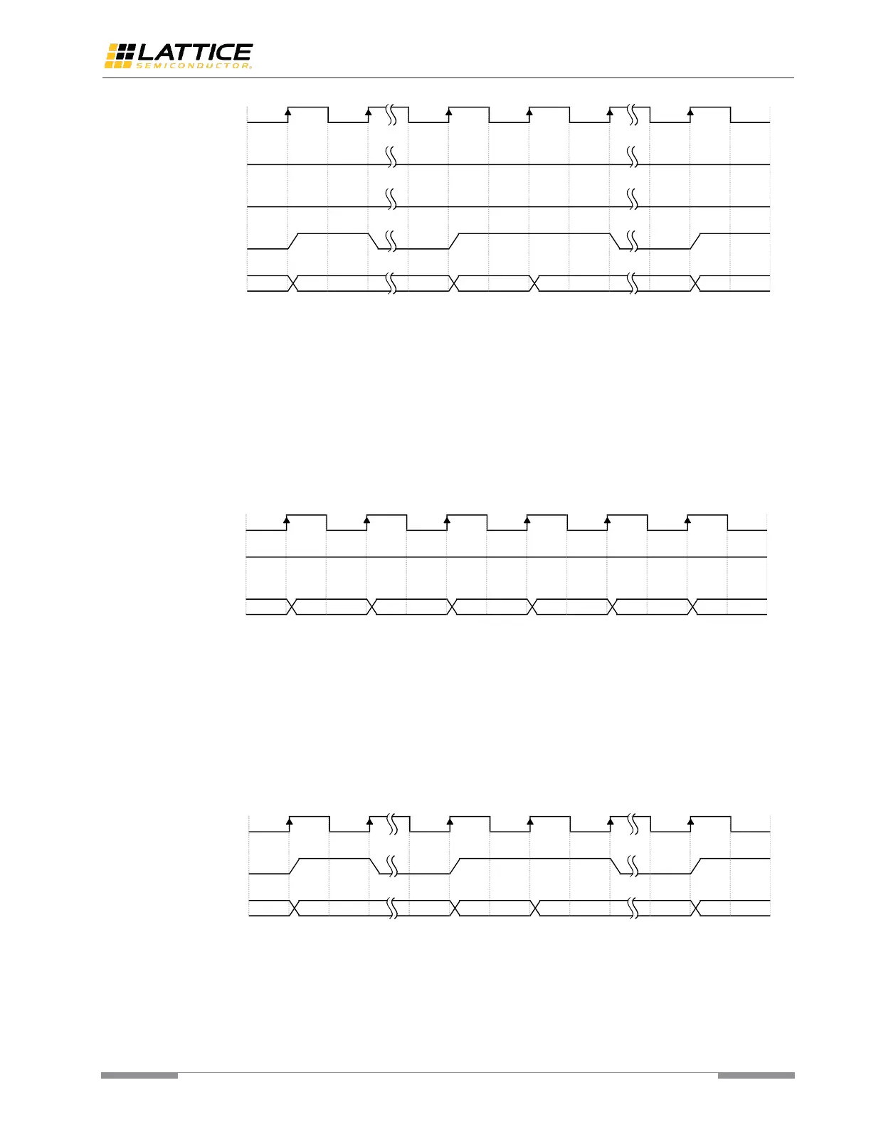
Figure 6.27. 64B/66B PCS Tx FIFO Write Operation Case II
Rx FIFO
The Rx FIFO module is implemented to adapt Rx path clock frequency and phase difference between 64B/66B PCS and
fabric. It also serves in following two application cases.
Case I (with GPLL)
In this case, GPLL is required to generate a 156.25MHz clock as the read clock of Rx FIFO. The rx_data_valid is
continuous because the bandwidth between the write side and read side is the same, 64bit@161.1328125MHz and
66bit@156.25MHz. Refer to Figure 6.28 for the timing diagram of this case. For more details about this clocking
scheme of this case, refer to the 64B/66B PCS with GPLL section.
Figure 6.28. 64B/66B PCS Rx FIFO Read Operation Case I
Case II (without GPLL)
In this case, user logic takes the clock originated from PMA as the read clock of Rx FIFO. The data valid signal for the
data out of Rx FIFO becomes discontinuous, considering that the frequency of write clock and read clock is the same
but the bandwidth between the write side and the read side is different. The write side should be adapted to the
bandwidth of 64B/66B Decoder module, 64bit@161.1328125MHz, and the read side is 64bit@161.1328MHz. Refer to
Figure 6.29 for the timing diagram of this case. For more details about this clocking scheme of this case, refer to the
64B/66B PCS without GPLL section.
Figure 6.29. 64B/66B PCS Rx FIFO Read Operation Case II
The Rx FIFO also implements Clock Tolerance Compensation (CTC) functionality to compensate clock frequency up to ±
100 PPM difference. This functionality can compensate up to 1 clock cycle difference every 5000 clock cycles in Rx path
by monitoring Rx FIFO status and inserting or deleting characters specified by IEEE802.3, if pre-defined criteria is met.
What should be noted is that this CTC functionality can only be used in the case with GPLL.
 Loading...