EasyManuals Logo

Lattice Semiconductor CertusPro-NX Usage Guide

Default Icon
171 pages
To Next Page IconTo Next Page
To Previous Page IconTo Previous Page
Page #76 background imageLoading...
Page #76 background image
CertusPro-NX SerDes/PCS Usage Guide
Preliminary Technical Note
76 © 2020-2021 Lattice Semiconductor FPGA-TN-02245-0.81
All rights reserved. CONFIDENTIAL
Clock
Direction
Description
Clocks within a Quad
tx_lalign_clk
N/A
This is a common clock shared by channels within Quad.
It is used in multiple-channel application cases. In Tx path, a common clock is used to
align all channels in order to minimize the lane-to-lane skew.
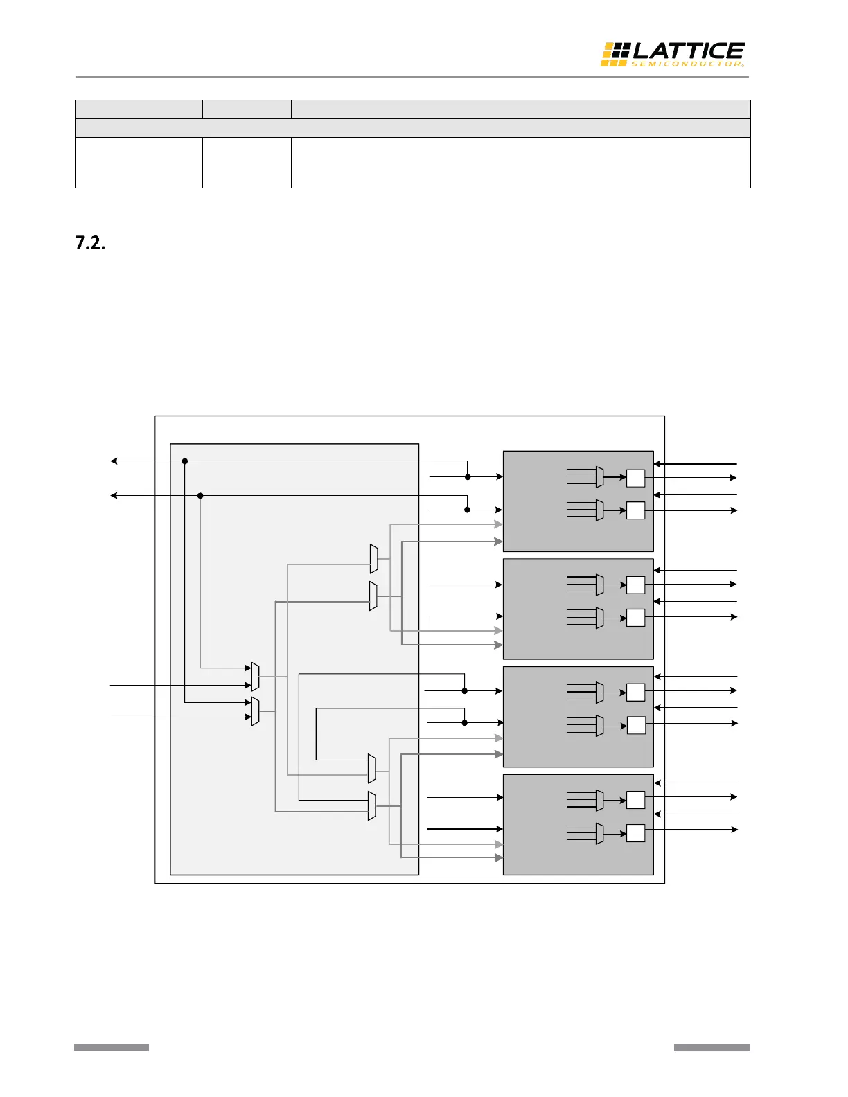
MPCS Quad Clock Detail
This section describes the clock distribution inside one Quad in detail. Figure 7.4 shows MPCS Quad clock distribution
diagram. Table 7.4 is the detailed Quad clock description. The Quad Common module implements the clock
multiplexing and distributing functionalities for multiple-channel applications.
The tx_pcs_clk and rx_pcs_clk from channel 0 are connected to Quad Common module and outside of MPCS Quad. The
tx_pcs_clk[0] and rx_pcs_clk[0] can be connected to all four channels inside the Quad. The tx_pcs_clk and rx_pcs_clk
from channel 2 are connected to Quad Common module, too, but tx_pcs_clk[2] and rx_pcs_clk[2] can be connected to
channel 2 and channel 3 only by Quad Common module. These clock connections bring some limitation on the
implementation for multiple-channel applications. Check the Quad Common section for more details.
/2,
/1
/2,
/1
Channel_0
Quad Common
MPCS Quad
tx_lalign_clk_in
rx_lalign_clk_in
tx_lalign_clk_out
rx_lalign_clk_out
tx_pcs_clk[0]
rx_pcs_clk[0]
tx_lalign_clk[0]
rx_lalign_clk[0]
tx_pcs_clk[1]
rx_pcs_clk[1]
tx_lalign_clk[1]
rx_lalign_clk[1]
tx_pcs_clk[2]
rx_pcs_clk[2]
tx_lalign_clk[2]
rx_lalign_clk[2]
tx_pcs_clk[3]
rx_pcs_clk[3]
tx_lalign_clk[3]
rx_lalign_clk[3]
Channel_1
/2,
/1
/2,
/1
Channel_2
Channel_3
/2,
/1
/2,
/1
/2,
/1
/2,
/1
tx_usr_clk[0]
tx_out_clk[0]
rx_usr_clk[0]
rx_out_clk[0]
tx_usr_clk[1]
tx_out_clk[1]
rx_usr_clk[1]
rx_out_clk[1]
tx_usr_clk[2]
tx_out_clk[2]
rx_usr_clk[2]
rx_out_clk[2]
tx_usr_clk[3]
tx_out_clk[3]
rx_usr_clk[3]
rx_out_clk[3]
Figure 7.4. Quad Clock Distribution Diagram

Table of Contents

Other manuals for Lattice Semiconductor CertusPro-NX

Questions and Answers:

Question and Answer IconNeed help?

Do you have a question about the Lattice Semiconductor CertusPro-NX and is the answer not in the manual?

Lattice Semiconductor CertusPro-NX Specifications

General IconGeneral
BrandLattice Semiconductor
ModelCertusPro-NX
CategoryComputer Hardware
LanguageEnglish