CertusPro-NX SerDes/PCS Usage Guide
Preliminary Technical Note
136 © 2020-2021 Lattice Semiconductor FPGA-TN-02245-0.81
All rights reserved. CONFIDENTIAL
8B/10B Encoder Interleave. Specifies whether the 8B/10B
Encoder Interleave is enabled or disabled.
1’b1 – enabled.
1’b0 – disabled.
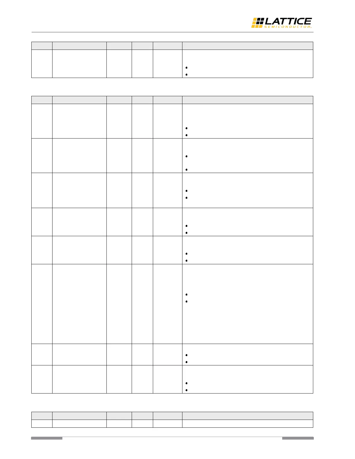
Table A. 34. Rx Path Control [reg20]
COMMA Byte alignment. Specifies the feature of putting
the COMMA byte to LSByte (Byte_0) of the data bus is
enabled or disabled.
1’b1 – disable this feature.
1’b0 – enable this feature.
Bond Mask. The banded channel mode is defined by
mc1_rx_bond_mode signal.
1’b1 – exclude this channel from bonded channel
group.
1’b0 – do not exclude this channel.
Bus Width. Specifies the internal data bus width for Rx
Path.
1’b1 – internal data bus is 20-bit width.
1’b0 – internal data bus is 10-bit width.
Note: this bit is not applicable for 64B/66B PCS mode.
8B/10B Decoding Enable. Specifies the 8B/10B decoding is
enabled or disabled.
1’b1 – decoding disabled.
1’b0 – decoding enabled.
Rx FIFO Enable. Specifies the Rx phase compensation FIFO
is enabled or disabled.
1’b1 – Rx phase compensation FIFO disabled.
1’b0 – Rx phase compensation FIFO enabled.
Gearing Enable. Specifies the 1:2 Gearing is enabled or
disabled. This bit controls the 8B/10B path and PMA Only
path gearing logic, as well as the “tx_out_clk” for all PCS
modes.
1’b1 – gearing is enabled.
1’b0 – gearing is disabled.
Note: In 8B/10B PCS mode and PMA Only mode, the
output clock (rx_out_clk) is driven by the divided-by-two
clock if this bit is set to “1”. In 64B/66B PCS mode, the
output clock (rx_out_clk) is driven by the clock with
doubled rate of default output clock, if this bit is set to
“1”.
Soft resets the Rx Path not including the register space.
1’b1 – reset the Rx MPCS path.
1’b0 – do not reset the Rx MPCS path.
Rx Path Enable. Specifies the MPCS channel Rx Path is
enabled or disabled.
1’b1 – MPCS channel Rx Path is disabled.
1’b0 – MPCS channel Rx Path is enabled.
Table A. 35. MPCS Rx Path Status [reg21]
 Loading...