CertusPro-NX SerDes/PCS Usage Guide
Preliminary Technical Note
70 © 2020-2021 Lattice Semiconductor FPGA-TN-02245-0.81
All rights reserved. CONFIDENTIAL
The “usr_dbus” is named as epcs_txdata_i in Tx path, or epcs_rxdata_o in Rx path.
The bit[0] is transmitted/received first.
Transfer ordering description:
T0: the first PMA clock cycle to capture/launch data in a data block transfer.
T1: the second PMA clock cycle to capture/launch data.
T2: the third PMA clock cycle to capture/launch data.
T3: the fourth PMA clock cycle to capture/launch data.
Quad Common
This per Quad module communicates with each channel within the Quad to implement the multiple lane alignment
function for both transmitter and receiver. It also talks to neighboring Quads to implement the lane alignment across
Quad boundary.
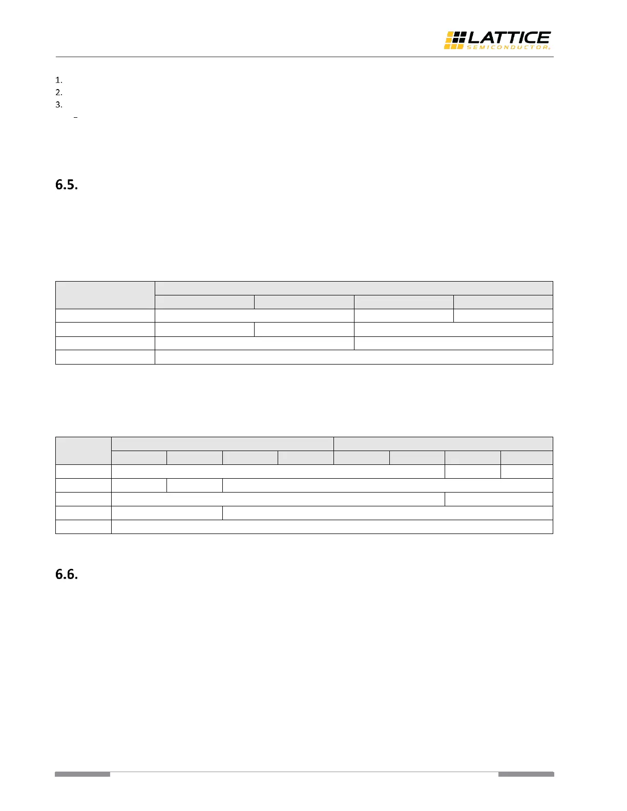
Within a Quad, the supported alignment modes are listed in Table 6.8. In Mode 1, Lane2 and Lane3 work
independently (not aligned). In Mode 2, Lane0 and Lane1 work independently (not aligned).
Table 6.8. Channel Alignment within One Quad
Together with adjacent Quad, this module supports up to 8-lane alignment. The allowed alignment modes are listed in
Table 6.9. Each of these two Quads supports all single Quad alignment modes. In Mode 5, Lane2 and Lane3 in Quad_1
work independently (not aligned). In Mode 6, Lane0 and Lane1 in Quad_0 work independently (not aligned).
Table 6.9. Channel Alignment between Two Quads
Reference Clock
All four PMA channels inside one Quad share the same reference clock source. This reference clock can source from
per-quad package pins (SDQx_REFCLKP/N), GPLL output and dedicated two package pins (SD_EXT0_REFCLKP/N and
SD_EXT1_REFCLKP/N). Refer to Figure 6.31 for the block diagram of reference clock source per quad.
 Loading...