CertusPro-NX SerDes/PCS Usage Guide
Preliminary Technical Note
FPGA-TN-02245-0.81 © 2020-2021 Lattice Semiconductor 47
All rights reserved. CONFIDENTIAL
SerDes/PCS Function Description
CertusPro-NX devices have one to three Quads of embedded SerDes/PCS logic. Each Quad, in turn, supports four
independent full-duplex data channels. A single channel can support a data link, and each Quad can support up to four
such channels.
The embedded SerDes CDR PLLs and Tx PLLs support data rates that cover a wide range of industry standard protocols.
SerDes (PMA)
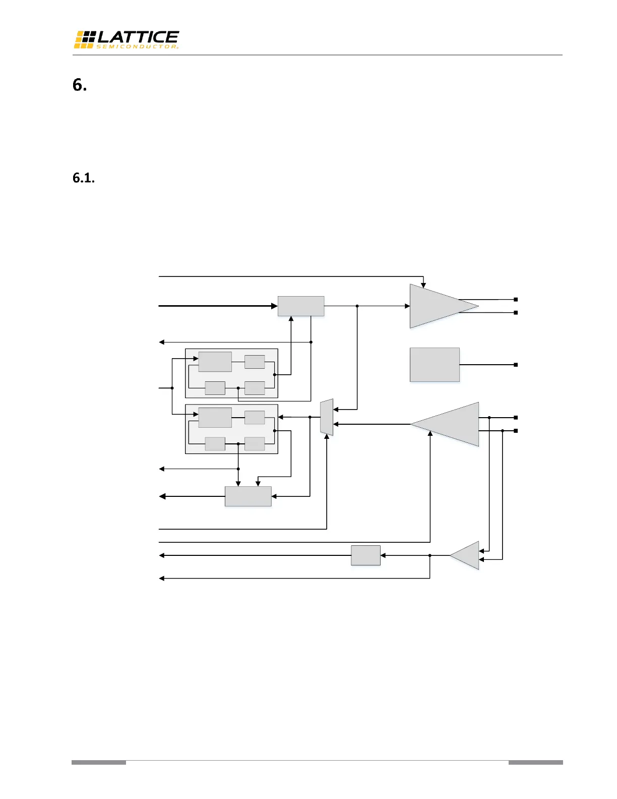
Figure 6.1 shows a simplified functional block diagram of the SerDes (PMA) macro. Each of the SerDes macros includes
three main sub-functions, Transmitter (Tx), Receiver (Rx), and PLL Clock blocks. The Tx block receives 5, 8, 10, 16, or 20
bits of transition-encoded data synchronous with a Tx clock, serializes it into a single stream of differential transmitted
data and transmits to the lane. The transmitter supports multi-level output driver, multi-level transition emphasis, and
multi-level Common Mode levels.
Figure 6.1. Simplified Block Diagram of the SerDes (PMA)
Output amplitude control range nominally spans from V
diff_pp
= 0 to V
diff_pp
= VCCSDx nominal, with a 1/128 typical
resolution at full-scale. A 3-tap FIR based Tx equalizer is implemented to support de-emphasis and pre-shoot. The
de-emphasis control range nominally spans from 0dB to beyond 20dB. Pre-cursor and post-cursor coefficients are
negative, with each coefficient able to be quantized to typically 1/128 resolution with respect to normalized full-scale.
The Rx block receives the serialized data from the lane, de-serializes this into a 5, 8, 10, 16, or 20 bits digital data and
provides the de-serialized data and the recovered link clock. An Rx continuous time linear equalizer (CTLE) is provided
with programmable gain and a single tap decision feedback equalization circuit (DFE) is provided with programmable
tap weight.
 Loading...