CertusPro-NX SerDes/PCS Usage Guide
Preliminary Technical Note
48 © 2020-2021 Lattice Semiconductor FPGA-TN-02245-0.81
All rights reserved. CONFIDENTIAL
The SerDes includes an eye monitor to map the post-equalized eye density. Eye X and Y coordinates can be controlled,
and the error density can be calculated at each coordinate. The X coordinate can be set by a 6-bit bus in 1.5mVdiff
(minimum) increments with a separate sign bit, and the Y coordinate by a 6-bit bus in UI/64 increments.
The PLL Clock blocks generate the required Tx and Rx link clocks and high frequency internal clocks from the provided
reference clock source, and contain all the control-feedback loops. Multiple single-lane macros may be formed into
wider transmit and/or receive links with support from the PCS as required by the relevant standards.
AC Coupling
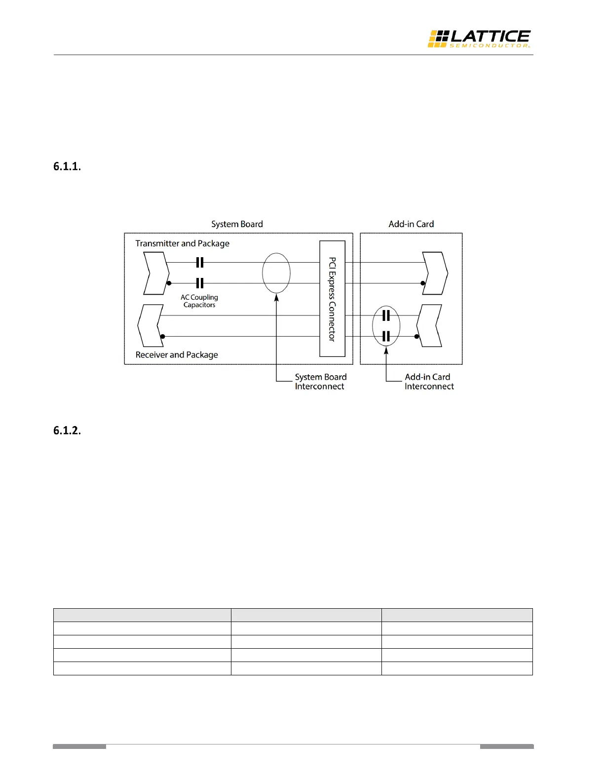
For most serial protocols, each PMA channel needs to be AC coupled externally. Suitable values for AC coupling
capacitors have to be used to maximize link signal quality, and conform to respective standards specifications.
Take PCI Express as example, the AC coupling capacitors should be placed near Tx side (Figure 6.2).
Figure 6.2. PCI Express AC Coupling Capacitors Location
PLL Clock Setting
Tx and Rx rates can be different frequencies, but limited to certain allowed integer ratios. The architecture of Tx PLL
and CDR PLL is similar. You can configure PLL VCO frequency F
VCO
, PMA internal clock frequency F
bit
, and PMA parallel
output clock frequency F
PMA
by accessing related PMA registers.
Following equation shows the relationship between F
VCO
, F
bit
, F
PMA
, and PMA reference clock frequency F
Ref
. For detailed
PLL setting for specific protocols, refer to the Clock Frequency section. M can be set as 1, 2, 4, and 8; F can be set as 1,
2, 3, 4, 5, and 6; N can be set as 5, 8, 10, 16, and 20.
Table 6.1 shows the operation range for PMA reference clock frequency F
Ref
, PLL VCO frequency F
VCO
, PMA internal
clock frequency F
bit
, and PMA parallel output clock frequency F
PMA
.
Table 6.1. Operation Range for F
Ref
, F
VCO
, F
bit
, and F
PMA
 Loading...