CertusPro-NX SerDes/PCS Usage Guide
Preliminary Technical Note
FPGA-TN-02245-0.81 © 2020-2021 Lattice Semiconductor 107
All rights reserved. CONFIDENTIAL
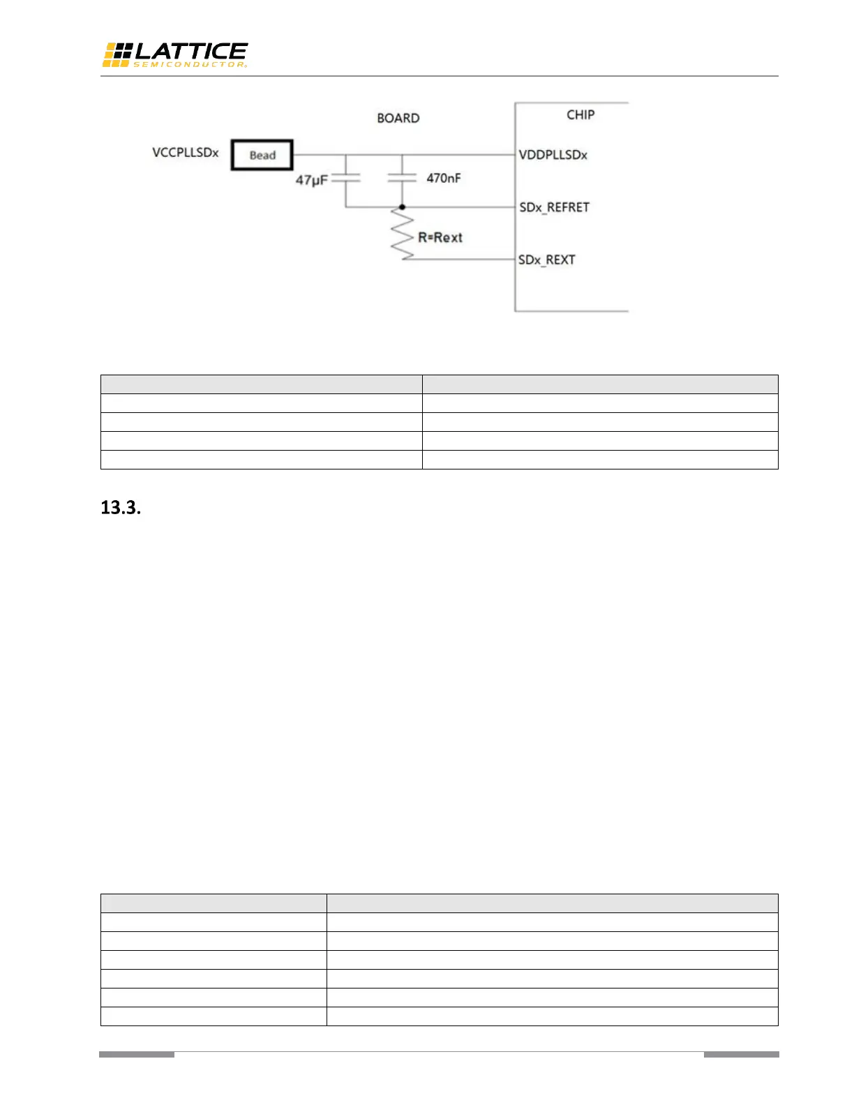
Figure 13.1. Example Connection to Analog Power and Reference Pins
Table 13.1. Recommended External Reference Resistor for Serval Differential Impedance Applications
Reference Clock Source Selection
The reference clock can source from per-quad package pins (SDQx_REFCLKP/N), GPLL output and dedicated two
package pins (SD_EXT0_REFCLKP/N and SD_EXT1_REFCLKP/N). However, there are some design considerations on the
selection of reference clock source for specific applications.
When clock from GPLL output is used as the reference clock for CertusPro-NX SerDes/PCS, the reference clock to the
GPLL should be assigned to the dedicated GPLL input pad. However, the GPLL output jitter may not meet system
specifications at higher data rates. Reference clock source from GPLL output is not recommended in jitter-sensitive
applications.
In PCI Express Hard IP mode, the reference clock source from per-quad package pins (SDQx_REFCLKP/N) need be used.
In PCI Express PIPE mode, the reference clock source from per-quad package pins (SDQx_REFCLKP/N) is also
recommended when the number of lane is not lager than four.
For applications with more than four lanes, the reference clock source from one of the two dedicated package pins
(SD_EXT0_REFCLKP/N or SD_EXT1_REFCLKP/N) is recommended.
For applications with several different speed grades and the frequency of the reference clock is different, there are two
solutions for reference sourcing. The first one is to use two reference clock sources with dynamic selection. The other
one is to use the reference clock source from GPLL, and the frequency of the GPLL output clock should be reconfigured
dynamically.
The reference clock is selected dynamically by a clock MUX block. Table 13.2 shows the usage of this clock MUX
primitive (PCSREFMUX). When PCSREFMUX is enabled, CertusPro-NX SerDes/PCS chooses the output clock of
PCSREFMUX instead of the default clock source from per-quad package pins (SDQx_REFCLKP/N).
Table 13.2. PCSREFMUX Usage
 Loading...