CertusPro-NX SerDes/PCS Usage Guide
Preliminary Technical Note
FPGA-TN-02245-0.81 © 2020-2021 Lattice Semiconductor 73
All rights reserved. CONFIDENTIAL
synchronous to this clock.
This clock is a node of fabric clock tree. The data received by user logic from MPCS is
synchronous to this clock.
This clock drives most part of Tx path logics. It may come from tx_pcs_clk in single-
channel application or from tx_lalign_clk in multiple-channel application where all
channels need to be aligned.
This clock has the same frequency as tx_pcs_clka or half frequency of tx_pcs_clka,
depending on input data rate and bus width. This clock and tx_pcs_clka are positive
edge aligned, with as little skew as possible between them so that output data from
this clock domain can be sampled by tx_pcs_clka directly.
This clock may come from rx_lalign_clk, a common clock for all channels in a
multi-channel application case. In that case, all channels may need to be aligned before
performing clock frequency compensation. In single-channel application, this clock is
derived from rx_pcs_clk.
This clock drives channel alignment logic and the write side of Elastic Buffer.
This clock may come from rx_pcs_clka, if the Elastic Buffer is bypassed. When Elastic
Buffer is enabled, the source of this clock can be tx_pcs_clk that comes from the Tx
path of the same channel, or tx_lalign_clk which is the common clock within bonded
channels. rx_pcs_clka is used in single-channel case, and tx_pcs_clk is for
multiple-channel usage.
This is a common clock shared by channels within Quad.
It is used in multiple-channel application cases. In Tx path, a common clock is used to
align all channels in order to minimize the lane-to-lane skew. In Rx path, this common
clock is used as local clock to perform clock frequency compensation.
This is a common clock shared by channels within Quad.
It is used in multiple-channel application cases. In Rx path, a common clock is required
to perform channel alignment as well as clock frequency compensation.
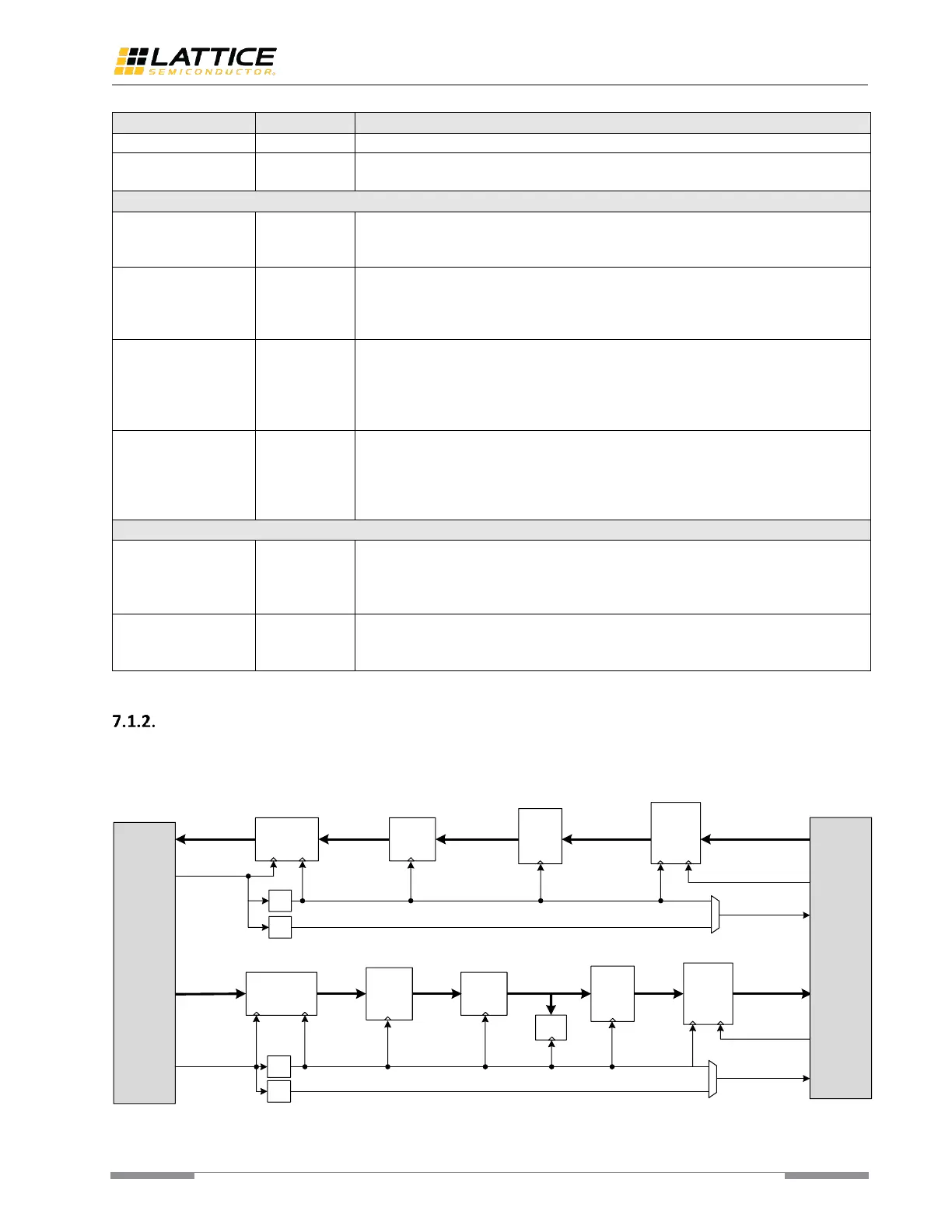
64B/66B PCS Clock
Figure 7.2 shows the 64B/66B PCS Channel clock diagram. Table 7.2 shows the 64B/66B PCS Channel clock detailed
descriptions.
Rx
Gear Box
Block
Aligner
De-
Scrambler
64B/66B
Decoder
Rx FIFO
Tx
FIFO
64B/66B
Encoder
Scrambler
Tx
Gear Box
16b data
TX Path
RX Path
PMA
/4
/4
BER
Monitor
User Logic
(Fabric)
66b block
2b sync
+ 64b data
8b TXC
+ 64b TXD
8b TXC
+ 64b TXD
16b data
66b block
2b sync
+ 64b data
2b sync
+ 64b data
8b RXC
+ 64b RXD
8b RXC
+ 64b RXD
tx_pcs_clk
(644.5MHz,
from Tx PLL)
tx_pcs_divclk (161.1328MHz)
tx_usr_clk
tx_out_clk
(161.1328MHz)
defaults
rx_pcs_clk
(644.5MHz,
from Rx CDR)
rx_usr_clk
rx_out_clk
(161.1328MHz)
defaults
rx_pcs_divclk (161.1328MHz)
rx_pcs_bufclk (322.2656MHz)
/2
tx_pcs_bufclk (322.2656MHz)
/2
Figure 7.2. 64B/66B PCS Channel Clock Diagram
 Loading...