CertusPro-NX SerDes/PCS Usage Guide
Preliminary Technical Note
144 © 2020-2021 Lattice Semiconductor FPGA-TN-02245-0.81
All rights reserved. CONFIDENTIAL
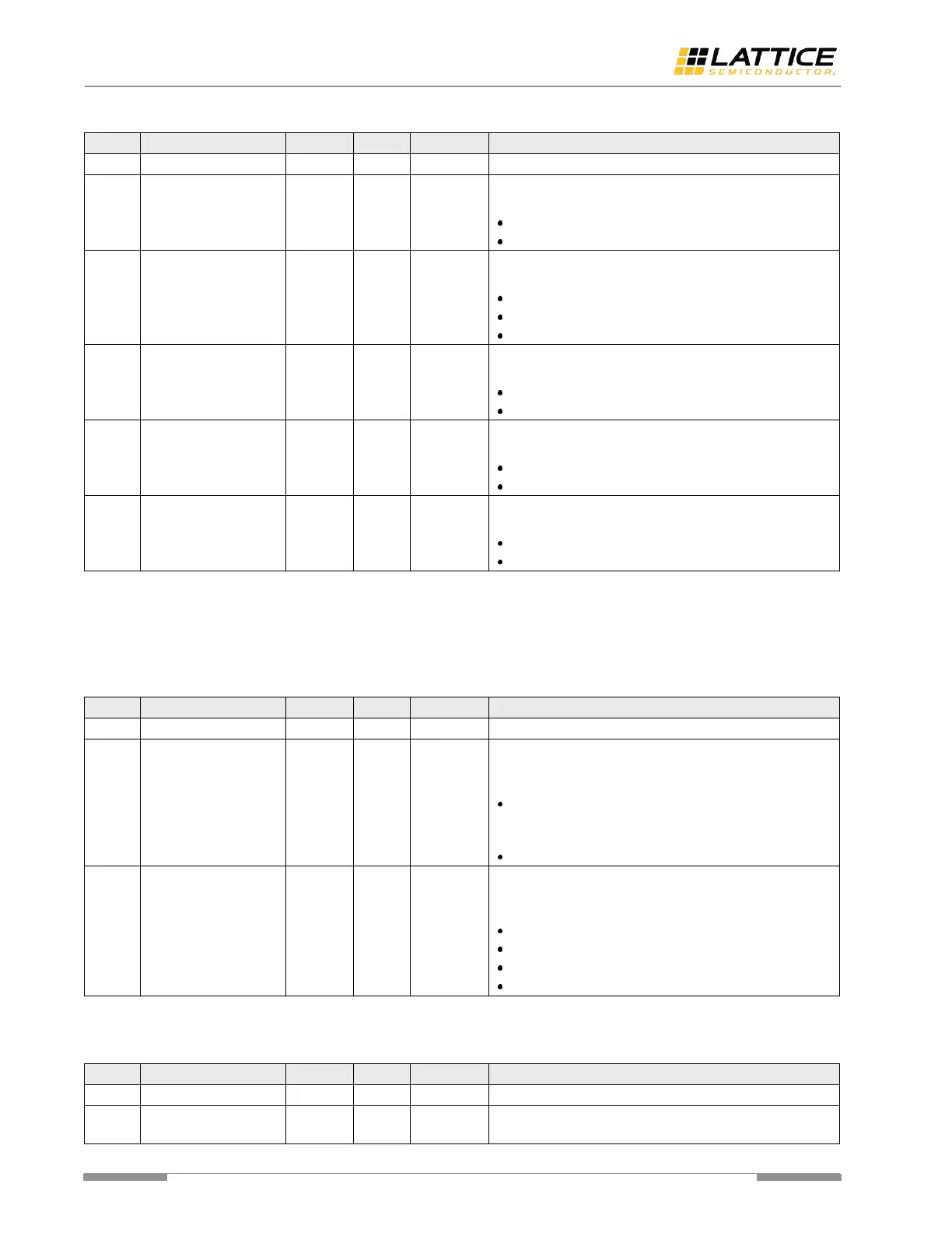
Table A. 80. Clock Frequency Compensation Control [reg60]
Enable Secondary Skip. Specifies the secondary skip
pattern is enabled or disabled.
1’b1 – Pattern Matching is enabled.
1’b0 – Pattern Matching is disabled.
Skip Pattern Length. Specifies the skip pattern length in
bytes.
2’b1x – 4-byte.
2’b01 – 2-byte.
2’b00 – 1-byte.
Clock Compensation Coding Mode. Specifies the clock
compensation coding scheme for the input data.
1’b1 – input data is in 10b code mode.
1’b0 – input data is in 8b code mode.
Clock Compensation FIFO. Specifies the Clock
Compensation FIFO is enabled or disabled.
1’b1 – Clock Compensation FIFO is enabled.
1’b0 – Clock Compensation FIFO is disabled.
Enable Clock Frequency Compensation. Specifies the clock
frequency compensation is enabled or disabled.
1’b1 – Clock Frequency Compensation is disabled.
1’b0 – Clock Frequency Compensation is enabled.
Note: The combination of “ctc_fifo_en” and “clk_comp_en” are listed below: {ctc_fifo_en, clk_comp_en}
2’b0x – bypass the input date of this module.
2’b10 – the module works as asynchronous FIFO without clock frequency compensation.
2’b11 – the module performs clock frequency compensation function.
Table A. 81. SKIP Pattern Insertion/Deletion Control [reg61]
Clock Correction Frequency Control. It defines the
minimum number of clock cycles between two clock
correction events, including SKIP deletion and insertion.
x(x=1 to 31) – The next time of SKIP deletion or
insertion must be x clock cycles away from the current
SKIP deletion or insertion.
1’b0 – on constraint on SKIP deletion and insertion.
Minimum SKIP pattern count. Used to guarantee the
minimum number of bytes between packets (that is the
minimum Inter Packet Gap) after SKIP deletion.
2’b11 – at least three SKIP pattern is kept in IPG.
2’b10 – at least two SKIP pattern is kept in IPG.
2’b01 – at least one SKIP pattern is kept in IPG.
2’b00 – no constraint on SKIP deletion.
Note: The length in byte of SKIP pattern is defined in “skp_ptn_len” domain register “Clock Frequency Compensation Control”.
Table A. 82. Elastic FIFO High Water Line [reg62]
Specifies the Clock Compensation FIFO high water line.
Mean is 5’b10000.
 Loading...