6.4.1.2. Rx Channel Data Transfer
Signals of Fabric-MPCS Rx channel interface fall into two categories:
Signals “rx_errdisp”, “rx_errcode”, “skp_add” and “skp_del” are strictly synchronous to the data bus (“rx_data”).
These signals indicate that “disparity error”, “code error”, “added SKIP pattern” and “deleted SKIP pattern” belong
to relative byte of data, separately.
Other signals are not aligned to a certain byte of data, for example, FIFO empty and full. However, these signals
last at least one clock cycle so that user logic can correctly sample them.
6.4.1.3. Tx Channel Data Transfer
Signals of Fabric-MPCS Tx channel interface fall into two categories:
Signals “tx_frcdisp”, “tx_dispval”, and “tx_frcdata” are strictly synchronous to the data bus (“tx_data”). These
signals are used to force disparity, reverse disparity, and force data to the exact corresponding byte of data.
Other signals are not aligned to a certain byte of data, for example, FIFO empty and full. However, these signals
last at least one clock cycle so that user logic can correctly sample them.
6.4.1.4. Function Block Description
Tx FIFO
The Tx FIFO module serves two purposes:
Provide user logic input data with 2:1 gearing to internal MPCS data path.
Clock phase compensation FIFO to ease MPCS-Fabric interface timing closure.
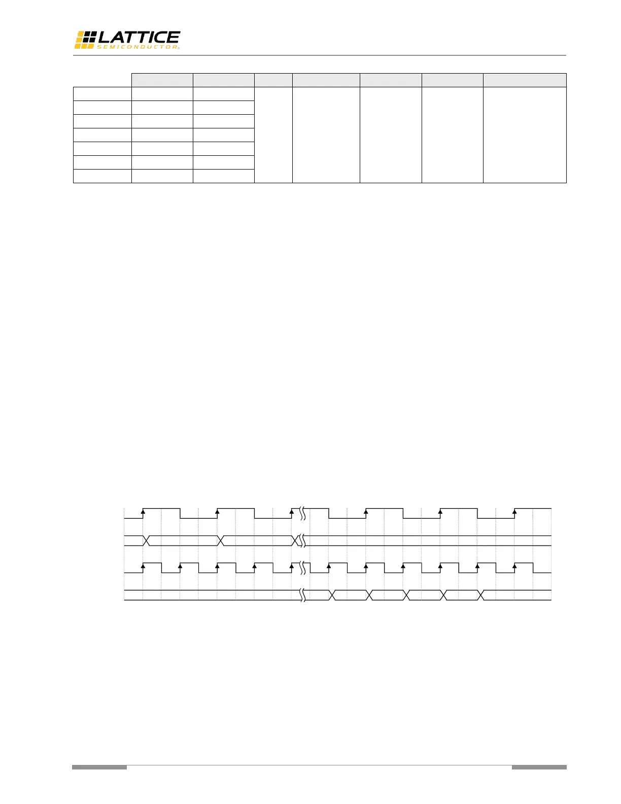
The 2:1 gearing can be optionally enabled to convert 4-byte data to 2-byte. Figure 6.6 shows how this conversion
proceeds.
Figure 6.6. Tx Gearing Case I
The 2:1 gearing logic can also be used to convert 2-byte data to 1-byte. Figure 6.7 shows how this conversion proceeds.
 Loading...