CertusPro-NX SerDes/PCS Usage Guide
Preliminary Technical Note
FPGA-TN-02245-0.81 © 2020-2021 Lattice Semiconductor 27
All rights reserved. CONFIDENTIAL
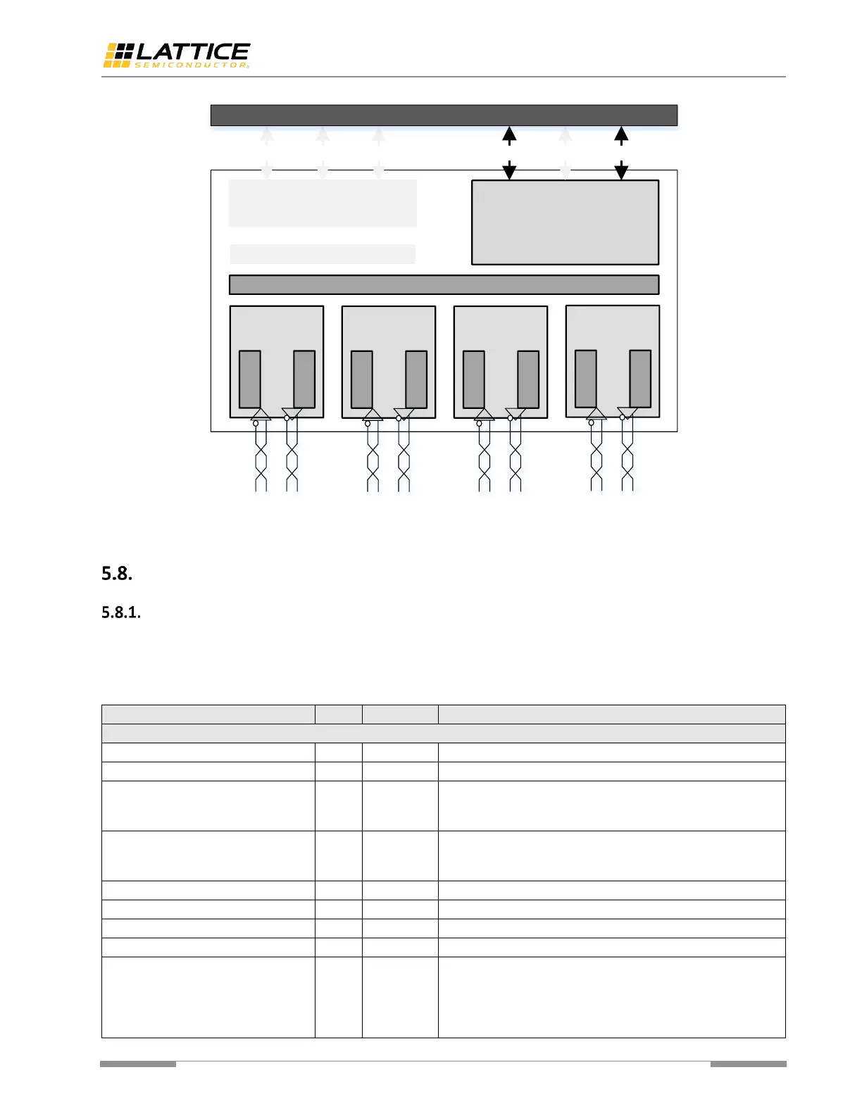
PCI Express Link Layer (x1 + x4)
MPCS x4
LMMI TLP
UCFG
LMMI MPCS EPCS
FPGA Core
PCI Express PCS
PMA Controller
PMA (SERDES)
Channel 0
Rx CDR
Tx PLL
PMA (SERDES)
Channel 1
Rx CDR
Tx PLL
PMA (SERDES)
Channel 2
Rx CDR
Tx PLL
PMA (SERDES)
Channel 3
Rx CDR
Tx PLL
Figure 5.11. PMA Only Mode
Detailed Interface Descriptions
MPCS Interface
MPCS interface is accessible when SerDes/PCS is configured as MPCS mode. MPCS mode is designed for applications
other than PCIe or PMA Only modes. Table 5.7 shows the detailed MPCS interface descriptions. All the signals listed in
this table are per lane, and NL means the number of lanes.
Table 5.7. MPCS Interface
User interface Rx clock input.
User interface Tx clock input.
Active low signal used to reset the Tx path of MPCS module.
This signal must be released only when PMA has completed
calibration.
Active low signal used to reset the Rx path of MPCS module.
This signal must be released only when PMA has completed
calibration.
Input clock for Clock Frequency Compensation. CTC clock input.
Fundamental reset. Triggers PCS auto calibration.
This low speed clock drives all calibration logic inside PMA
Controller. Connecting this clock port to mpcs_tx_out_clk_o is
recommended, and the recommended frequency range is
100-300 MHz. This clock should be stable and continuous after
power on.
 Loading...