CertusPro-NX SerDes/PCS Usage Guide
Preliminary Technical Note
78 © 2020-2021 Lattice Semiconductor FPGA-TN-02245-0.81
All rights reserved. CONFIDENTIAL
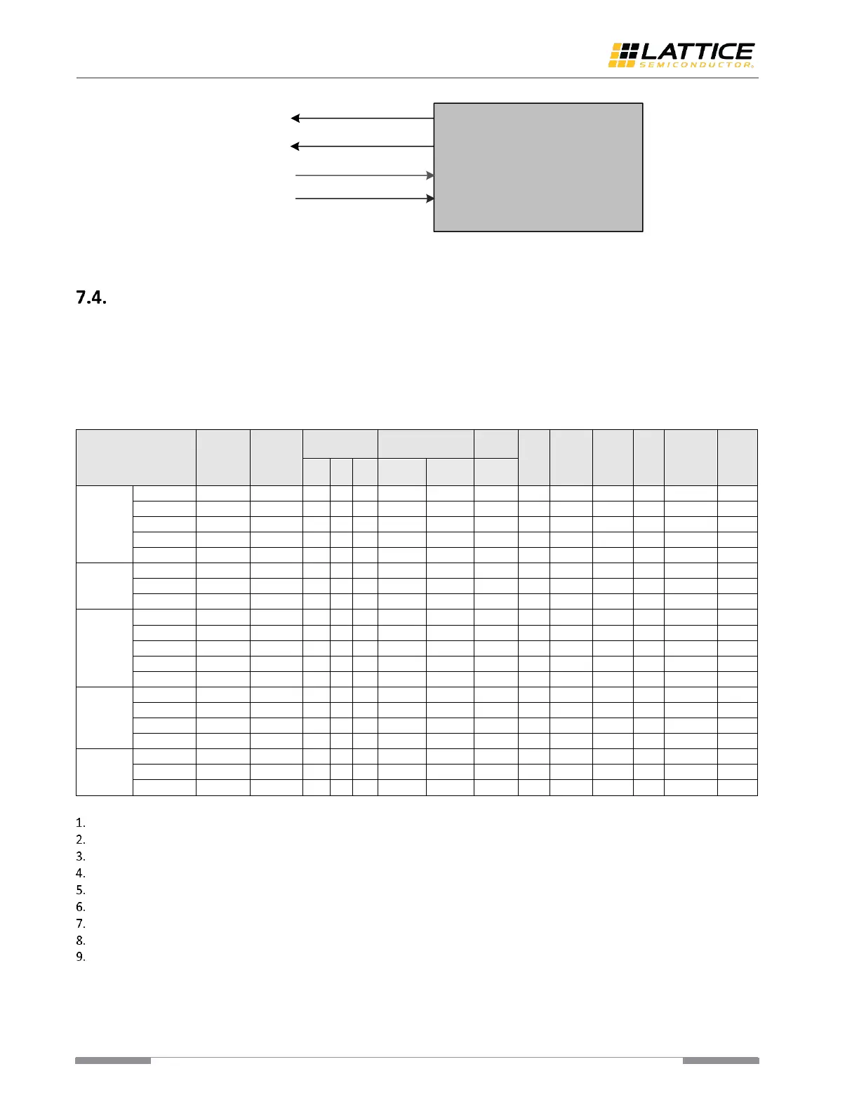
Quad 0
Floating
(internally gated)
Floating
(internally gated)
rx_lalign_clk_in[0]
tx_lalign_clk_in[0]
rx_lalign_clk_out[0]
tx_lalign_clk_out[0]
Tie High/Low
Tie High/Low
Figure 7.6. Single Quad Clock Connection
Clock Frequency
This section lists the recommended reference clock frequency, the PLL settings, PMA/PCS internal clock frequency,
interface data bus width and clock frequency for Ethernet, SLVS-EC, CoaXPress, DP/eDP and PCIe protocols. Refer to
Table 7.5 for the recommended settings for these protocols.
The PLL settings are the same for Tx PLL and Rx CDR, considering that the architecture of Tx PLL and Rx CDR is similar.
Refer to the SerDes (PMA) section for the Tx PLL and Rx CDR implementation details inside PMA channel.
Table 7.5. Recommend Settings for Some Protocols
Notes:
M can be set as 1, 2, 4 and 8.
F can be set as 1, 2, 3, 4, 5 and 6.
N can be set as 5, 8, 10, 16 and 20.
F
VCO
=F
Ref
*M*F*N
F
bit
=F
Ref
*F*N
F
PMA
=F
Ref
*F
F
PCS
presents the clock frequency of tx_pcs_clk and rx_pcs_clk.
F
OUT
presents the clock frequency of tx_out_clk and rx_out_clk.
The setting in this row is applicable to the whole range of this baud rate. The actual bit rate is determined by the reference
clock, which can vary in a small range.
 Loading...