CertusPro-NX SerDes/PCS Usage Guide
Preliminary Technical Note
FPGA-TN-02245-0.81 © 2020-2021 Lattice Semiconductor 81
All rights reserved. CONFIDENTIAL
8B/10B PCS Multiple Lane Tx Path
Case III-a: Use Tx FIFO
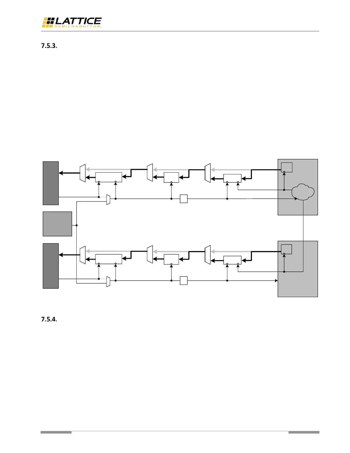
As shown in Figure 7.12, the tx_pcs_clk0 and tx_pcs_clk1 are the generated clock from the corresponding channel PMA
Tx PLL. Tx FIFO modules are enabled to eliminate the clock phase difference between tx_usr_clk and each channel
internal clock (tx_out_clk0 and tx_out_clk1). The tx_out_clk0 is used to drive FPGA global clock tree, and a leaf node of
this clock tree returning to MPCS is used as the read clock of Tx FIFO.
However, an uncertain one clock cycle latency is introduced by Tx FIFO module. A common clock (tx_lalign_clk) from
Quad Common module is used by all lanes to replace tx_pcs_clk to drive the Tx path. The Tx Lane-to-lane Deskew
module works as asynchronous FIFO to eliminate this uncertain latency and the clock phase difference between
tx_lalign_clk and tx_pcs_clk.
Figure 7.12 shows the two-lane application. The clock structure of multiple-lane applications (more than two) is similar
to this two-lane application.
Figure 7.12. Case III-a Clock Structure
8B/10B PCS Multiple Lane Rx Path
Case IV-a: Bypass Elastic Buffer
As shown in Figure 7.13, the rx_pcs_clk0 and rx_pcs_clk1 are the recovered clock from the corresponding channel PMA
Rx CDR. Rx FIFO modules are enabled to eliminate the clock phase difference between rx_usr_clk and each channel
internal clock (rx_out_clk0 and rx_out_clk1). The rx_out_clk0 is used to drive FPGA global clock tree, and a leaf node of
this clock tree returning to MPCS is used as the read clock of Rx FIFO.
The rx_lalign_clk from Quad Common module is used by all lanes to replace each channel rx_pcs_clk to drive the Rx
path. The Lane Aligner modules are enabled for Rx lane-to-lane Deskew and for eliminating the phase difference
between rx_pcs_clk and rx_lalign_clk.
Elatstic Buffer module is bypassed, considering no frequency difference between rx_pcs_clka and rx_usr_clk.
Figure 7.13 shows the two-lane application. The clock structure of multiple-lane applications (more than two) is similar
to this two-lane application.
 Loading...