RTC
®
5 PC Interface Board
Rev. 1.9 e
2 Product Overview
29
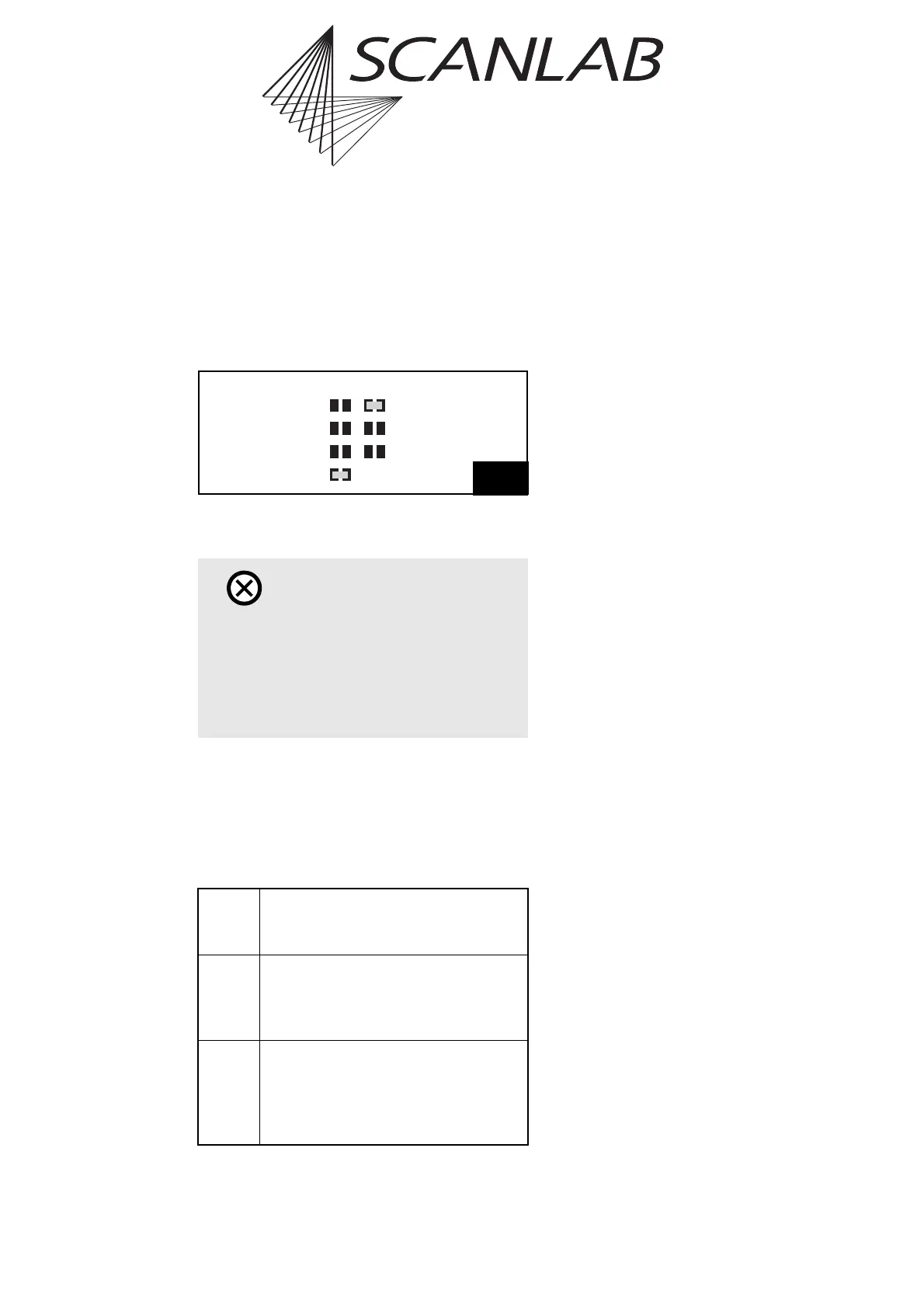
pin (17). Alternatively, each of the two pins can be set
permanently to +5 V (HIGH) or to GND (LOW level).
Alternatively, pin (17) can be configured for the
LATCH signal by closing the correspondingly labeled
jumper. Figure 1 shows an example jumper configu-
ration assigning DATA7 to pin (15) and the LATCH
signal to pin (17).
2.4.3 Type Identification
The RTC
®
5’s ID number reveals the board’s factory-
equipped jumper configuration. The jumper configu-
ration is additionally encoded in a three-digit type
code scheme:
Examples:
• “Type 000”: all jumpers open
• “Type 124”: JP1 in position 1-2 (5 V signal level),
JP3 closed (DATA7 at pin 15),
JP8 closed (LATCH at pin 17)
2.5 Optional Accessories
In addition to the RTC
®
5 PC interface board and its
software package, the following accessories can be
obtained from SCANLAB (only hardware extensions
from SCANLAB should be used in combination with
the RTC
®
5):
2.5.1 XY2-100 Converter
SCANLAB’s XY2-100 converter allows the RTC
®
5
board to control scan systems equipped with a
conventional XY2-100 interface (see page 42).
2.5.2 Data Cables
To connect the RTC
®
5 board to scan systems,
SCANLAB offers appropriate cables in a variety of
lengths – either conventional cables for electrical data
transfer or polymer optical fiber cables or optical data
transfer (see page 44).
2.5.3 Laser Adapter
SCANLAB offers an laser adapter which can be
plugged into the RTC
®
5’s 15-pin LASER connector.
This adapter’s 9-pin female D-SUB connector
provides the same signals and pin-out as the RTC
®
4’s
9-pin laser connector (see page 48).
2.5.4 PCI Slot Covers
For connecting a second scan head or a Z axis to the
secondary scan head connector (10-pin connector
2. SCAN HEAD, see page 41), a suitable slot cover
with a 9-pin D-SUB connector is available from
SCANLAB (see page 42).
For using the inputs and signals of the
MARKING ON THE FLY connector (16-pin connector,
see page 51), a suitable slot cover with a 15-pin
D-SUB connector is available from SCANLAB (see
page 51).
Caution!
• Make sure that not more than one of the three
jumpers for pin (15) is closed. Also make sure
that not more than one of the four jumpers for
pin (17) is closed.
Closing more than one jumper for pin (15) or
(17) will damage the board’s electronics.
Digit 1 =0: Jumper JP1 open (no signal)
=1: Jumper JP1 in position 1-2 (5 V)
=2: Jumper JP1 in position 2-3 (3.3 V)
Digit 2
(relates
to pin
15)
=0: Jumper JP2-4 open (no signal)
=1: Jumper JP2 closed (+5 V)
=2: Jumper JP3 closed (DATA7)
=3: Jumper JP4 closed (GND)
Digit 3
(relates
to pin
17)
=0: Jumper JP5-8 open (no signal)
=1: Jumper JP5 closed (+5 V)
=2: Jumper JP6 closed (DATA7)
=3: Jumper JP7 closed (GND)
=4: Jumper JP8 closed (LATCH)
Pin17 Pin15
Data7
Data7
+5V
+5V
GND
GND
Latch
(JP2)
(JP3)
(JP4)
(JP5)
(JP6)
(JP7)
(JP8)
Example configuration for jumpers JP2-JP8:
Pin (15): DATA7, Pin (17): LATCH signal