RTC
®
5 PC Interface Board
Rev. 1.9 e
15 Appendix A: The RTC
®
5 PC/104-Plus Board
586
Jumper JP1: Selecting the Output Signal
Level at the MULTI connector
Via Jumper JP1 on the back side of the
RTC
®
5 PC/104-Plus board (see figure 62 on
page 578), the level of the MULTI connector’s 16-bit
digital output (pins A1, A3, A5, A7, A9, A11, A13,
A15, A17, A19, A21, A23, A25, A27, A29, A31),
LATCH signal (pin A33), SYNC signal (pin A34),
BUSY OUT signal (pin A36) and VCC_OUT signal (pin
A35) can be configured for 5 V or 3.3 V (also see
page 580). This corresponds to signal level selection
at the EXTENSION 1 connector of the
RTC
®
5 PC interface board (see page 49).
SCANLAB’s RTC
®
5 PC/104-Plus board is supplied in
various jumper configurations for JP1 (also see "Type
Identification", page 575).
Jumper 2-8: Configuring Pin B40 and Pin B42
at the MULTI connector
Pins B40 and B42 of the MULTI connector can be
configured via jumpers JP2-JP8 on the back side of
the RTC
®
5 PC/104-Plus board (see figure 62 on
page 578 and page 580). This corresponds to the
configuration possibilities at pins (15) and (17) of the
RTC
®
5 PC interface board’s EXTENSION 2 connector
(see page 50).
The most significant bit (DATA7) of the 8-bit output
value can be assigned to pin B40 or pin B42. Alterna-
tively, each of the two pins can be set permanently to
+5 V (HIGH) or to GND (LOW level). Alternatively,
pin B42 can be configured for the LATCH signal by
closing the correspondingly labeled jumper.
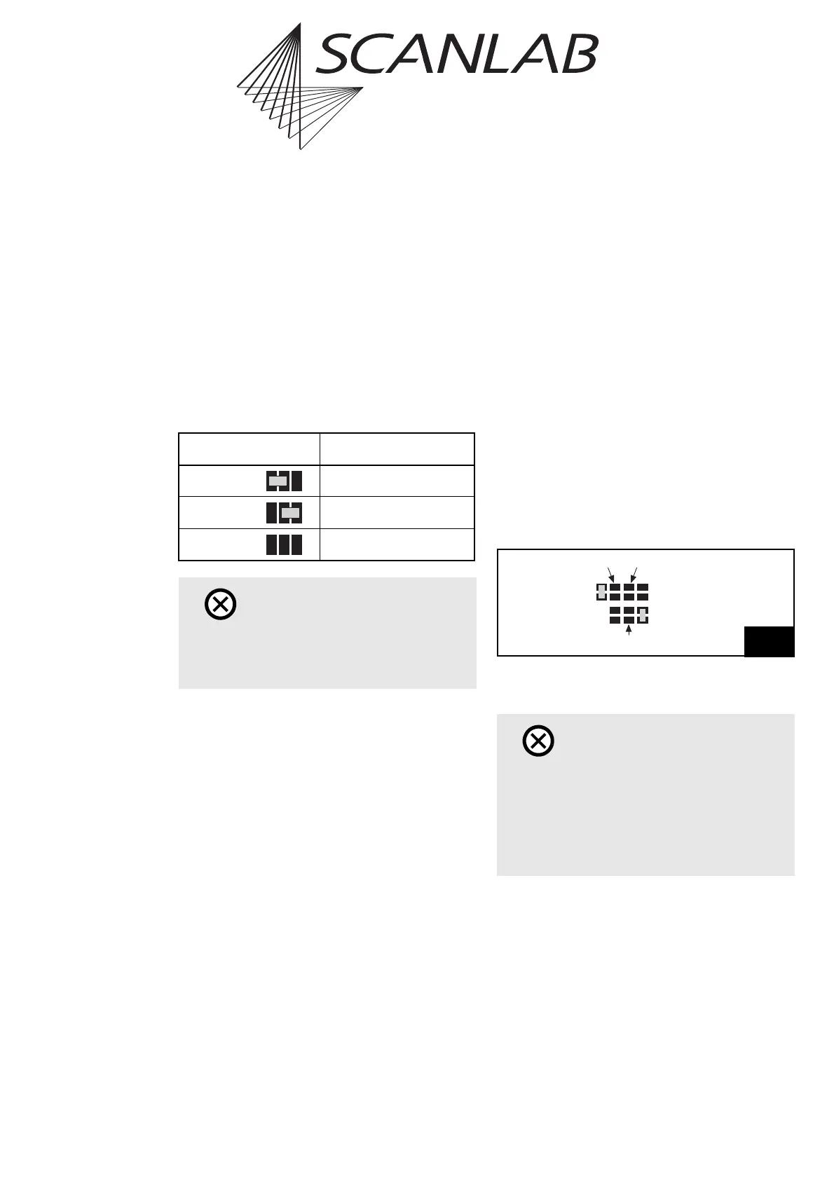
Figure 66 shows an example jumper configuration
assigning DATA7 to pin B40 and the LATCH signal to
pin B42
SCANLAB’s RTC
®
5 PC/104-Plus board is supplied in
various jumper configurations for JP2-JP8 (also see
"Type Identification", page 575).
Jumper JP1 Signal Level
Position 1-2 5V
Position 2-3 3.3 V
open no output signals
Caution!
• Be sure that not all three jumper pins are closed.
Otherwise, the board’s electronics will be
damaged.
Caution!
• Make sure that not more than one of the three
jumpers for pin B40 is closed. Also make sure
that not more than one of the four jumpers for
pin B42 is closed.
Closing more than one jumper for pin B40 or
B42 will damage the board’s electronics.
JP2(B40:+5V)
JP3(B40:Data7)
(B40:GND)JP4
JP6(B42:Data7)(B42:Latch)JP8
(B42:GND)JP7 JP5(B42:+5V)
Example configuration for jumpers JP2-JP8:
Pin B40: DATA7, Pin B42: LATCH signal