RTC
®
5 PC Interface Board
Rev. 1.9 e
4 Layout and Interfaces
48
Laser Adapter (Optional)
An optional laser adapter from SCANLAB can be
plugged into the RTC
®
5’s 15-pin LASER connector.
This adapter’s 9-pin female D-SUB connector
provides the same signals and pin-out as the RTC
®
4’s
9-pin laser connector.
Notes
• The laser adapter can not be directly plugged into
the RTC
®
5 if an XY2-100 converter is already
plugged in.
• The BUSY OUT signal, 2-bit digital input and 2-bit
digital output are not available at the laser
adapter’s 9-pin D-SUB connector.
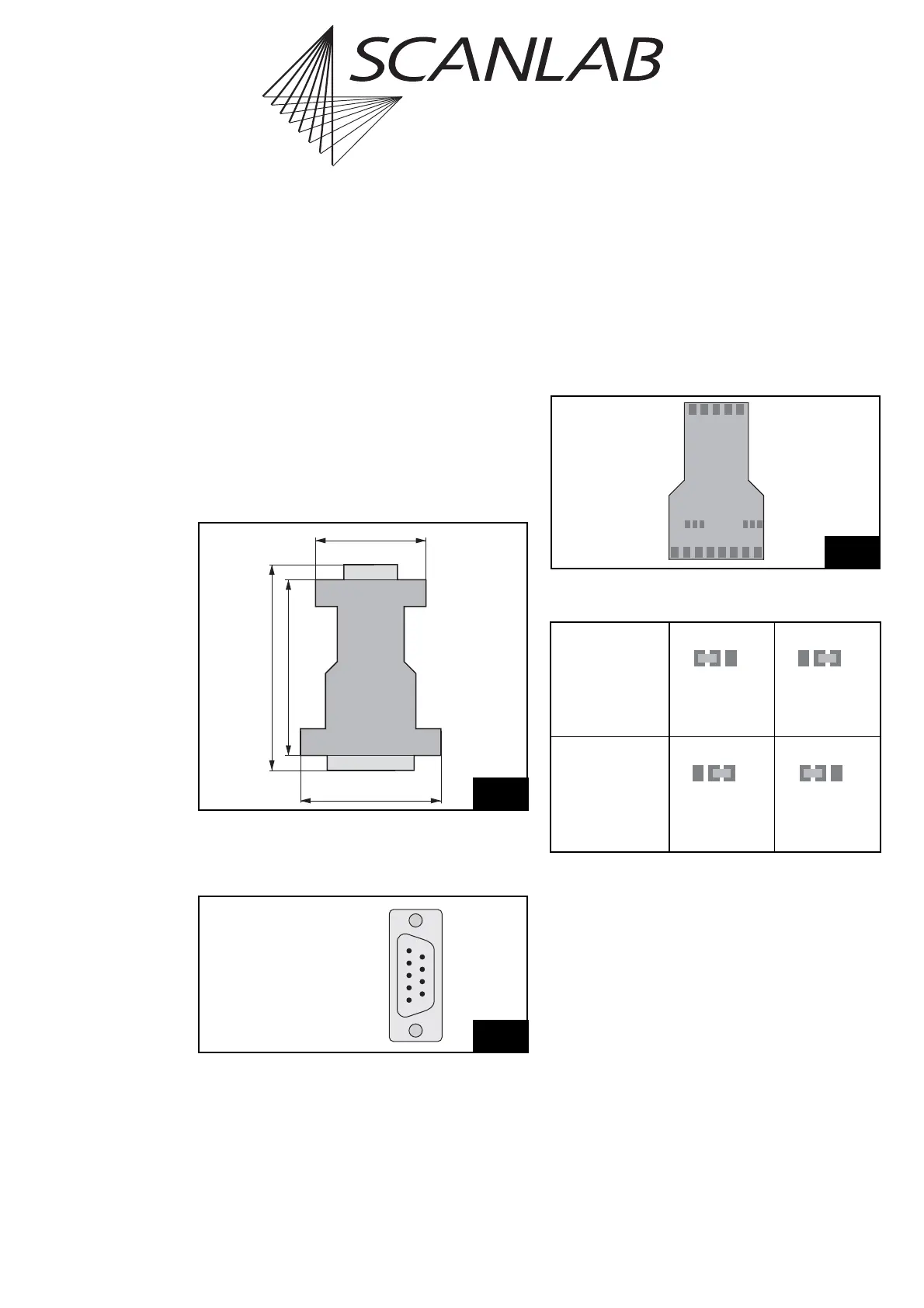
Figure 12 shows the dimensions of the laser adapter.
The pin-out of the 9-pin D-SUB connector is shown in
figure 13.
The signals at pins (2) and (4) of the 9-pin D-SUB
connector can be selected via two solder jumpers in
the laser adapter. To do so, carefully open the laser
adapter’s housing via its four clip latches (e.g. using
a screwdriver). The solder jumpers JP1 and JP2 are on
the laser adapter’s PCB, between the two D-SUB
connectors. Figure 14 shows the positions of the
jumpers on the PCB. The table below lists the possible
jumper settings and the corresponding signals.
42
33
52
62
Thickness
16
15-pin male D-Sub
9-pin female D-Sub
Dimensions of the optional laser adapter
13
(6) GND2
(7) GND2
(8) /START
(9) /STOP
LASER1 (1)
LASERON / ANALOG OUT2 *) (2)
LASER2 (3)
ANALOG OUT1 / +5 V * (4)
GND (5)
Pin-out of the laser adapter’s 9-pin female D-SUB connector
* dependent on the jumper configuration of the solder jumpers on
the laser adapter’s PCB
Jumper JP1
(signal at pin 2)
Position 1-2
LASERON
(standard
configuration)
Position 2-3
ANALOG OUT2
Jumper JP2
(signal at pin 4)
Position 1-2
ANALOG OUT1
(standard
configuration)
Position 2-3
+5 V
LON
PIN2
ANA2
+5V
PIN4
ANA1
JP2JP1
11
Positions of solder jumpers JP1 and JP2 on the laser adapter’s PCB