RTC
®
5 PC Interface Board
Rev. 1.9 e
15 Appendix A: The RTC
®
5 PC/104-Plus Board
584
15.3.2 Jumper Settings
Before installing the RTC
®
5 PC/104-Plus board in a
PC/104 stack, you might need to configure the
board’s jumpers. SCANLAB ships RTC
®
5 PC/104-Plus
boards in various jumper configurations (also see
"Type Identification", page 575). The jumpers are
soldered junctions and customers can subsequently
reconfigure them by using a soldering iron
If you do not want to change the factory settings,
proceed with "Installing the RTC
®
5 PC/104-Plus
Board", page 587.
Jumper 17+18: Setting the Binary Stack
Address
Jumpers JP17+JP18 on the back side of the
RTC
®
5 PC/104-Plus board (see figure 62 on
page 578) allow the board’s stack address to be
defined. You can thereby electrically customize the
board to its position in the PC/104 stack. SCANLAB
recommends assigning stack addresses as follows
(for an overview of PCI stack positions, see figure 67
on page 587):
Stack address configuration ensures that each
RTC
®
5 PC/104-Plus board in a stack gets to have one
of the four CLK, IDSEL, REQ and GNT signals of the
PCI bus explicitly assigned to it:
Selection of the REQ and GNT signals is only relevant
for bus master boards. RTC
®
5 PC/104-Plus boards are
target devices and therefore not dependent on
master stack positions.
A configured stack address corresponding to the PCI
stack position ensures optimal relationships between
the signal path lengths (which differ for each PCI
stack position). This results in stable PCI-bus transfer
of assigned signals.
Notes
• The RTC
®
5 PC/104-Plus board’s stack address is
factory-set to 0. If you install the board directly
onto a CPU board (without other modules in
between), then jumpers JP17+JP18 don’t need
to be changed.
Caution!
• When altering a jumper configuration, take
care not to damage the board’s electronics!
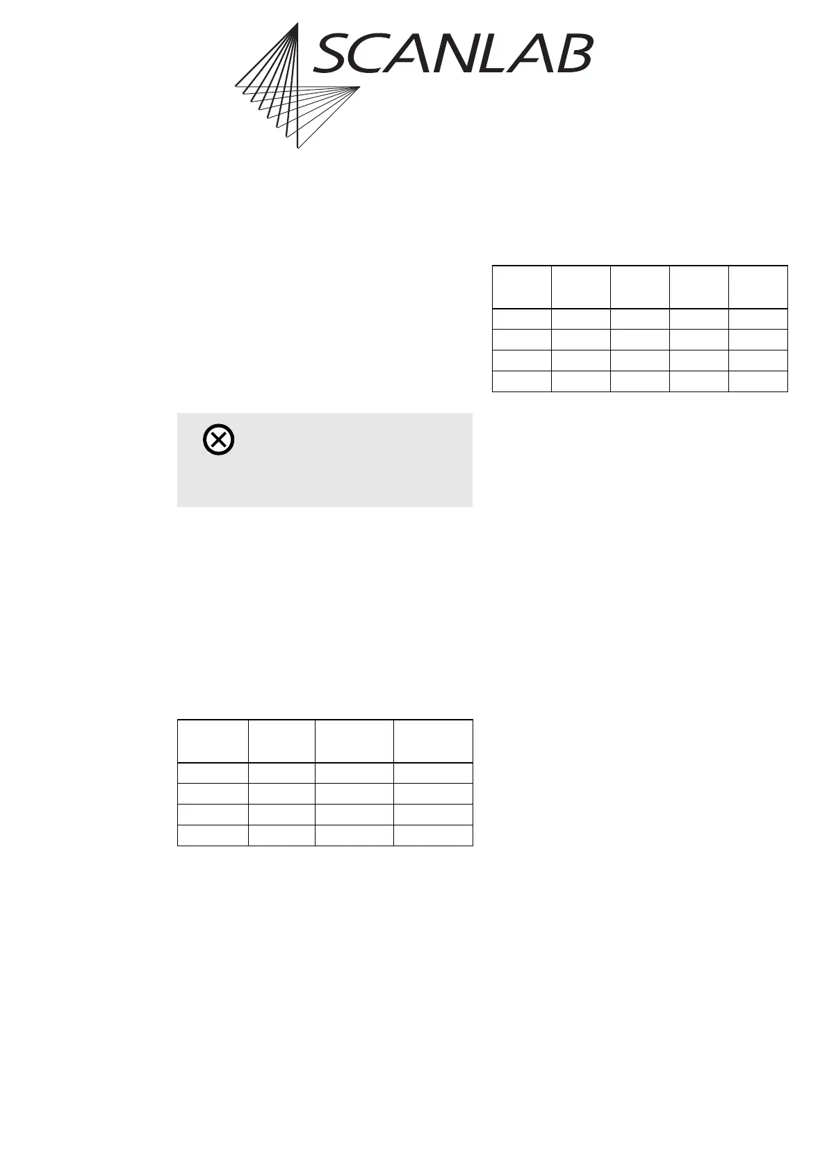
PCI stack
position
stack
address
JP17 JP18
1 0 * closed closed
2 1 closed open
3 2 open closed
4 3 open open
Stack
address
CLK IDSEL REQ GNT
0 CLK0 IDSEL0 REQ0 GNT0
1 CLK1 IDSEL1 REQ1 GNT1
2 CLK2 IDSEL2 REQ2 GNT2
3 CLK3 IDSEL3 REQ3 GNT3