AddressS 1 A
Data1 A
SCL
Stretch
Data2
A
DataN NA P
Master to Slave
Slave to Master
RS = Repeated Start
S = Start
A = Acknowledge
P = Stop
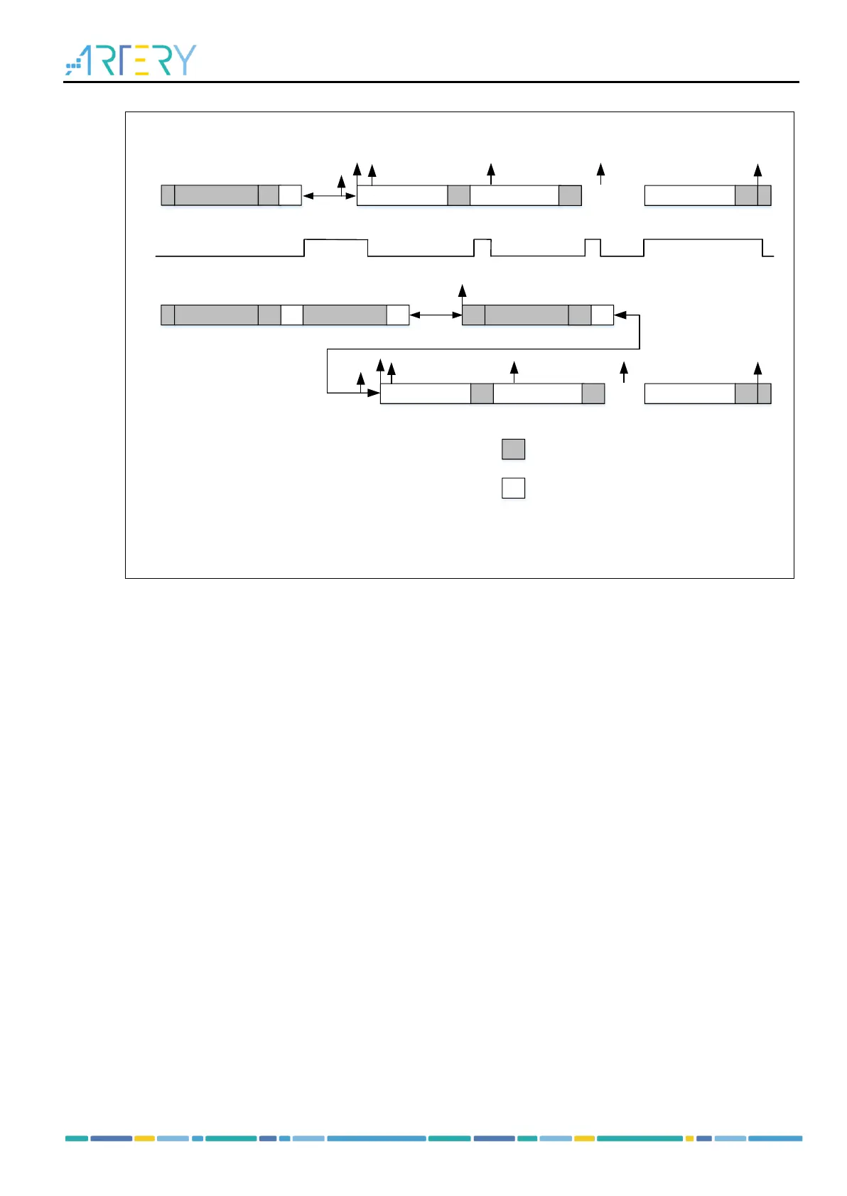
Example : I2C Slave transfer N bytes to I2C Master .
EV1. I2C_STS1_ADDR7F = 1, reading STS1 and then STS2 will clear the
event。
EV2. Both the internal shift register and the data register I2C_DT are empty,
I2C_STS1_TDBE = 1,the data is directly moved to the internal shift register
after Data1 is written.
EV3. I2C_DT write Data , I2C_STS1_TDBE = 0。
EV4. ACKFAIL = 1 , The I2C_STS1_ACKFAIL bit can be cleared by writing 0.
When a stop condition is detected,I2C_STS1_TDBE = 0。
EV1
EV2 EV3
EV4
...
TDBE
EV3 EV3
Address HeadS A Address A
EV1
Address HeadRS A
SCL
Stretch
EV1
Data1 A Data2
A
DataN NA P
EV2
EV3
EV4
...
EV3 EV3
SCL
Stretch
7-bit address
10-bit address
R/W
0
R/W
1
R/W
7-bit address mode:
1. Wait for the master to send an address
2. EV1: Address is matched (ADDR7F=1), and then the slave pulls the SCL bus low. Reading STS1
and then STS2 by software clears the ADDR7F bit. It then enters transmission stage, and both DT
register and internal shift register are now empty. The TDBE bit is set 1 by hardware.
3. EV2: When the data is written to the DT register, it is directly moved to the shift register and the
SCL bus is released. The TDBE bit is still set 1 at this time.
4. EV3: The DT register remains empty, but the shift register is not. Writing to the DT register
clears the TDBE bit.
5. EV4: After receiving the ACKFAIL event from the master, ACKFIAL=1 is activated. Writing 0 to the
ACKFIAL bit clears the event.
6. End of communication.
10-bit address mode:
1. Wait for the master to send an address
2. EV1: Address is matched (ADDR7F=1), and then the slave pulls the SCL bus low. Reading STS1
and then STS2 by software clears the ADDR7F bit. Wait for the master to re-send Start condition.
3. EV1: Address is matched (ADDR7F=1). Reading STS1 and then STS2 clears the ADDR7F bit
once more. It then enters transmission stage. Both DT register and shift register are empty. The
TDBE is set 1 by hardware.
4. EV2: When the data is written to DT register, it is directly moved to the shift register, and SCL bus
is released. The TDBE is still set 1 at this time.
5. EV3: The DT register remains empty but the shift register is not. Writing to the DT register
clears the TDBE bit.
6. EV4: After receiving the ACKFAIL event from the master, ACKFIAL=1 is activated. Writing 0 to the
ACKFIAL bit clears the event.
7. End of communication.