AT32F421 Series Reference Manual
2022.11.11 Page 63 Rev 2.02
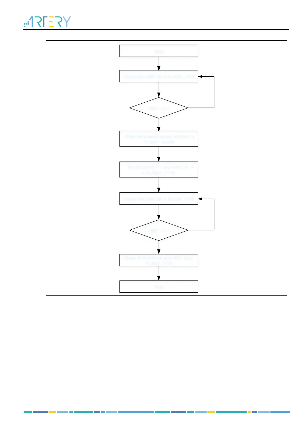
Figure 5-1 Flash memory sector erase process
Start
Write the erased sector address to
FLASH_ADDR
Set SECERS = 1 and ERSTR =1
in FLASH_CTRL
OBF = 0 ?
Check the OBF bit in FLASH_STS
Read EPPERR bit and ODF bit in
FLASH_STS
No
Yes
OBF = 0 ?
Check the OBF bit in FLASH_STS
No
Yes
End
Mass erase
Mass erase feature can erase the entire Flash memory.
To perform mass erase, follow the procedures below:
Check that no Flash memory operation is ongoing by checking the OBF bit in the FLASH_STS
register
Set the BANKERS and ERSTR bits in the FLASH_CTRL register to enable mass erase;
Wait until the OBF bit becomes “0” in the FLASH_STS register. Read the EPPERR bit and ODF bit
in the FLASH_STS register to verify.
Note:
1) When the boot memory is configured as the Flash memory extension area, performing mass-
erase operation erases automatically the entire Flash memory and its extension area.
2) Read access during erase operation halts the CPU until the completion of erase.
3) Internal HICK must be enabled prior to erase operation.