AT32F421 Series Reference Manual
2022.11.11 Page 68 Rev 2.02
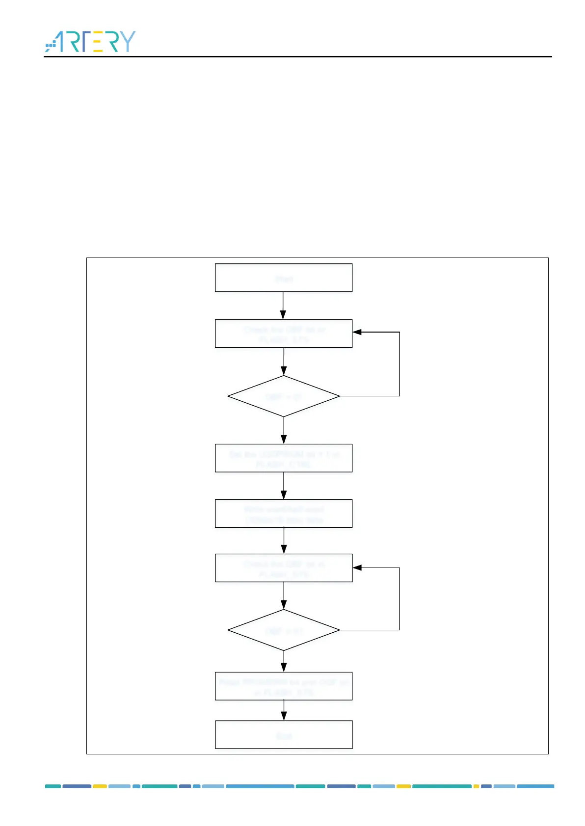
5.4.3 Programming operation
The User system data area can be programmed with 16-bit or 32-bit data at one time.
The following process is recommended:
Check that no Flash memory operation is ongoing by checking the OBF bit in the FLASH_STS
register
Set the USDPRGM bit in the FLASH_CTRL register, so that the programming instructions for the
user system data area can be received;
Write the data (half-word/word) to be programmed to the designated address;
Wait until the OBF bit in the FLASH_STS register becomes “0”, read the PRGMERR and ODF bit
to verify
Note: Read operation to the Flash memory during programming halts CPU until the completion of
programming. The internal HICK must be enabled prior to programming operation.
Figure 5-5 System data area programming process