AT32F421 Series Reference Manual
2022.11.11 Page 192 Rev 2.02
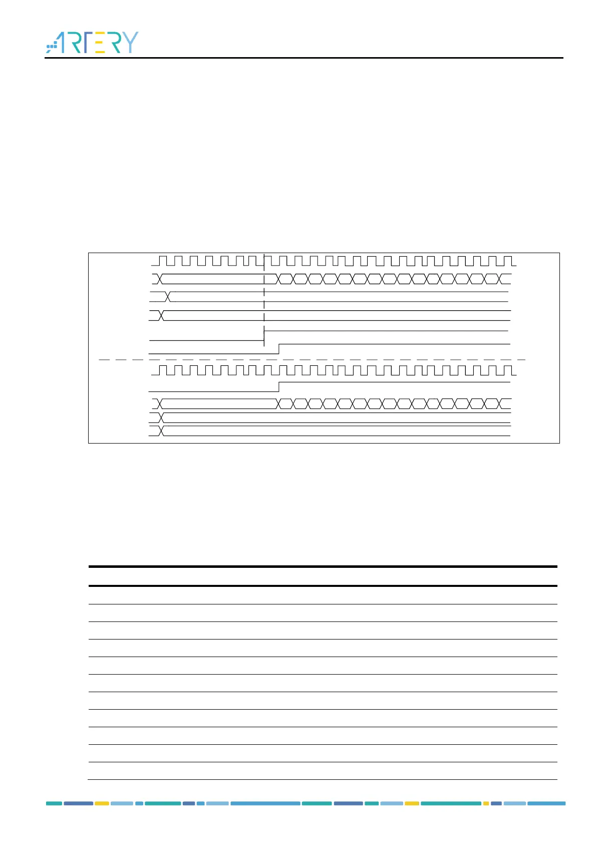
Starting master and slave timers synchronously by an external trigger:
In this example, configure the master timer as master/slave mode synchronously and enable its slave
timer synchronization function. This mode is used for synchronization between master timer and slave
timer.
Set the STS bit of the master timer.
Configure master timer output signal TRGOUT as an overflow event (PTOS[2: 0]=3’b010). The
master timer outputs a pulse signal at each counter overflow event, which is used as the
counting clock of the slave timer.
Configure the slave timer mode of the master timer as trigger mode, and select C1IN as trigger
source
Configure slave timer trigger input signal TRGIN as master timer output
Configure slave timer as trigger mode (SMSEL=3’b110 in the TMR2_STCTRL register)
Figure 14-37 Starting master and slave timers synchronously by an external trigger
14.2.3.6 Debug mode
When the microcontroller enters debug mode (Cortex
TM
-M4 core halted), the TMR3 counter stops
counting by setting the TMR3_PAUSE bit in the DEBUG module.
14.2.4 TMR3 registers
These peripheral registers must be accessed by word (32 bits).
TMR3 registers are mapped into a 16-bit addressable space.
Table 14-5 TMR3 register map and reset value