AT32F421 Series Reference Manual
2022.11.11 Page 39 Rev 2.02
3 Power control (PWC)
3.1 Introduction
For the AT32F421 series, its operating voltage supply is 2.6 V ~ 3.6 V, with a temperature range of -
40~+105
o
C. To reduce power consumption, this series provides three types of power saving modes,
including Sleep, Deepsleep and Standby modes so as to achieve the best trade-off among the conflicting
demands of CPU operating time, speed and power consumption. The AT32F421 series has two power
domains─VDD/VDDA domain and 1.2 V domain. The VDD/VDDA domain is supplied directly by external
power, while, the 1.2 V domain is powered by an embedded LDO in the VDD/VDDA domain.
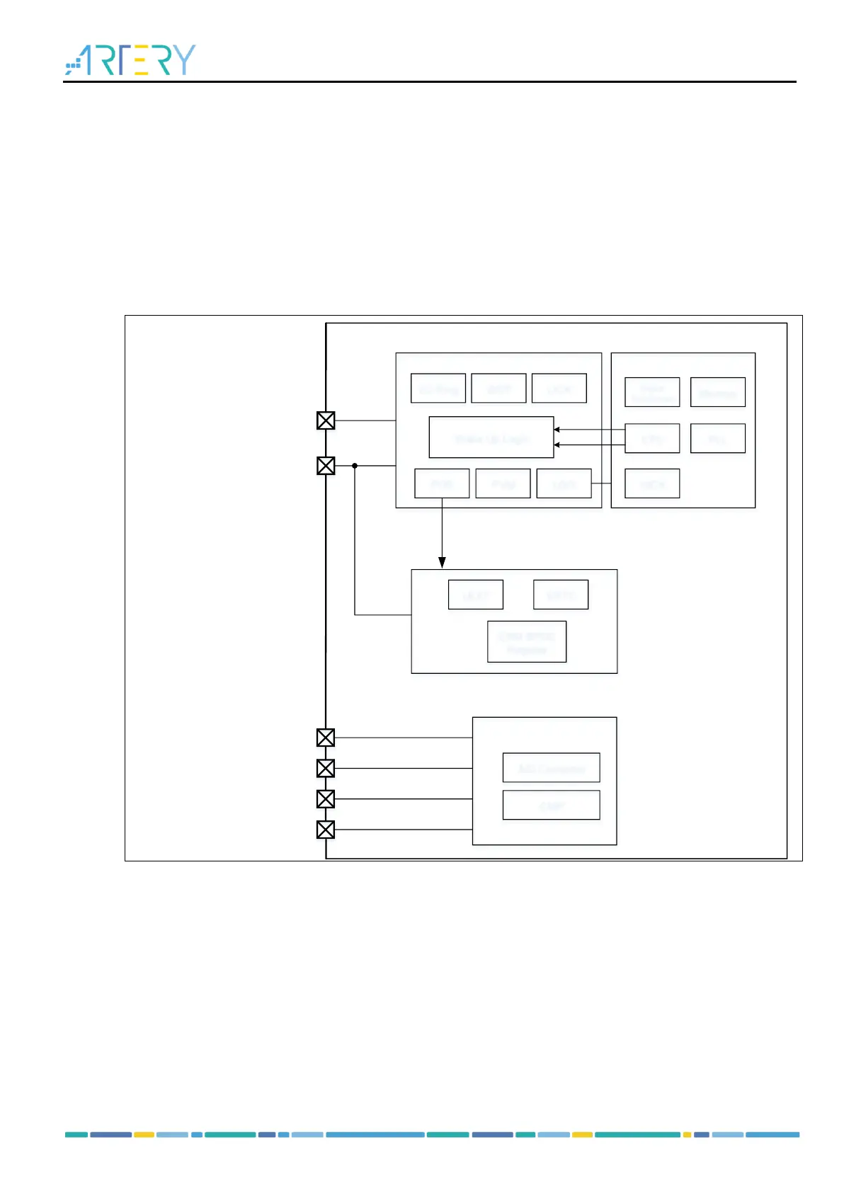
Figure 3-1 Block diagram of each power supply
3.2 Main Features
Two power domains: VDD/VDDA domain and 1.2 V core domain
Three types of power saving modes: Sleep mode, Deepsleep mode, and Standby mode
Internal voltage regulator supplies 1.2 V voltage for the core domain
Power voltage detector is provided to generate an interrupt or even when the supply voltage is
lower or higher than a programmed threshold
VDD/VDDA applies separated digital and analog module to reduce noise on external power