AT32F421 Series Reference Manual
2022.11.11 Page 64 Rev 2.02
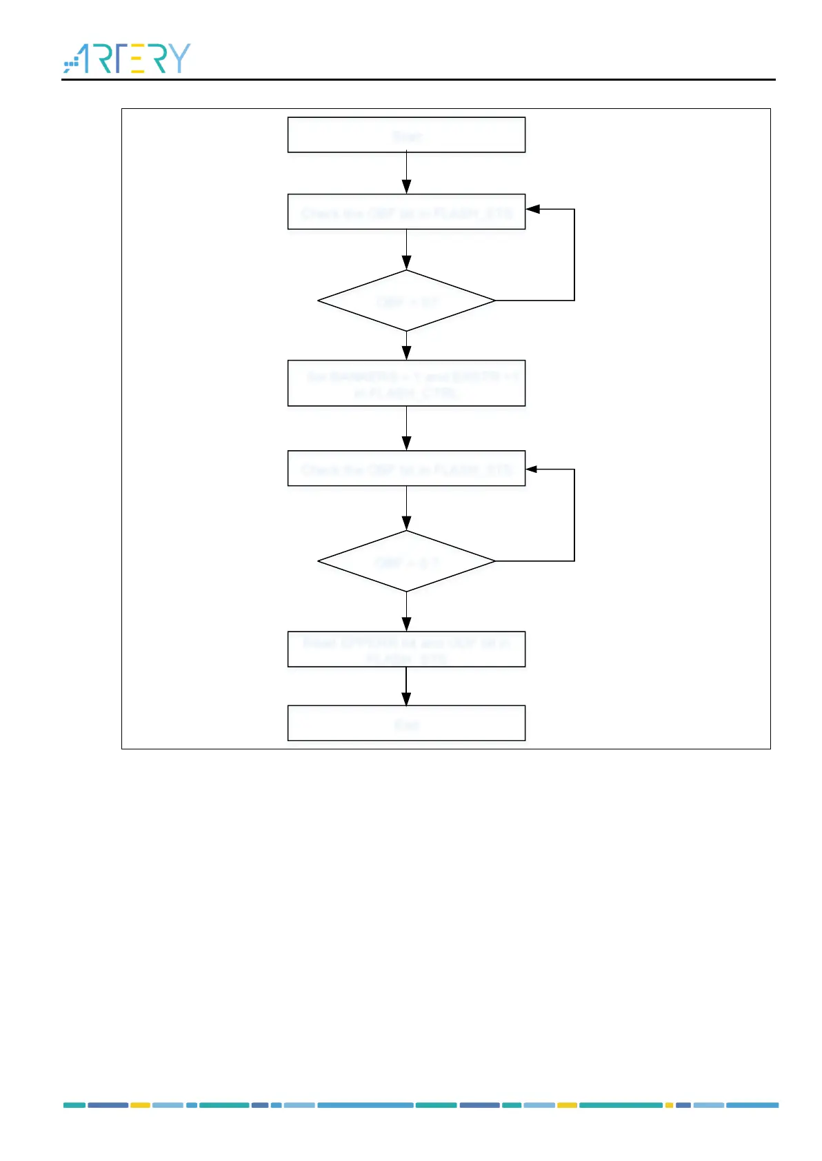
Figure 5-2 Flash memory mass erase process
Start
No
Check the OBF bit in FLASH_STS
OBF = 0?
Yes
Set BANKERS = 1 and ERSTR =1
in FLASH_CTRL
OBF = 0 ?
Check the OBF bit in FLASH_STS
Read EPPERR bit and ODF bit in
FLASH_STS
No
Yes
End
5.2.3 Programming operation
The Flash memory can be programmed with 32-bit, 16-bit or 8-bit data at one time.
The following process is recommended:
Check that no Flash memory operation is ongoing by checking the OBF bit in the FLASH_STS
register
Set the FPRGM bit in the FLASH_CTRL register, so that the Flash memory programming
instructions can be received;
Write the data (word/half-word/byte) to be programmed to the designated address;
Wait until the OBF bit in the FLASH_STS register becomes “0”, read the EPPERR, PRGMERR and
ODF bits to verify.
Note:
1. When the address to be written is not erased in advance, the programming operation is
not executed unless the data to be written is all 0. In this case, a programming error is reported
by setting the PRGMERR bit in the FLASH_STS register.
2. Read operation to the Flash memory during programming halts CPU until the completion of
programming.
3. Internal HICK must be enabled prior to programming.