NOTE
When the clock pinch board needs to be used, both the master and slave MPUs must be installed with a
clock pinch board.
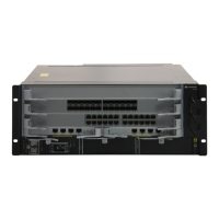
5.23.3 Interfaces
The CLM has two BITS interfaces, corresponding to the CLK1 and CLK2 interfaces on the main
control board. Table 5-131 describes the types and functions of the two BITS interfaces.
Table 5-131 Types and functions of the BITTS interfaces
Name Quantity Description
BITS0
Corresponds to
the CLK1
interface on the
main control
board.
1
The BITS0 interface can be configured as the input or
output interface.
l When functioning as the input interface, the BITS0
interface can receive the 2.048 MHz clock signal,
2.048 Mbit/s clock signal, 1 pulse per second (pps)
clock signal, or DC level shift (DCLS) code stream
from the upstream device and generate the 19.44
MHz clock signal for the system. The BITS0
interface can also obtain the time information and
provide the time information for LPUs.
l When functioning as the output interface, the
BITS0 interface can send the 2.048 MHz clock
signal, 2.048 Mbit/s clock signal, 1 pps clock
signal, or DC level shift (DCLS) code stream to the
downstream device.
BITS1
Corresponds to
the CLK2
interface on the
main control
board.
1
The functions are similar to the functions of the BITS0
interface.
5.23.4 Interface Attributes
Table 5-132 describes the attributes of the BITS interfaces.
Table 5-132 Attributes of the BITS interfaces
Attribute
Description
Connector type RJ45
5 Boards
Quidway S9300 Terabit Routing Switch
Hardware Description
5-100 Huawei Proprietary and Confidential
Copyright © Huawei Technologies Co., Ltd.
Issue 01 (2010-12-15)

 Loading...