8254
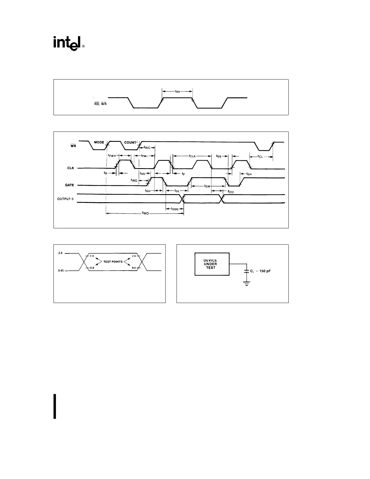
WAVEFORMS (Continued)
RECOVERY
231164–15
CLOCK AND GATE
231164–16
*Last byte of count being written.
A.C. TESTING INPUT, OUTPUT WAVEFORM
231164–17
A.C. Testing: Inputs are driven at 2.4V for a Logic ‘‘1’’ and 0.45V
for a Logic ‘‘0.’’ Timing measurements are made at 2.0V for a
Logic ‘‘1’’ and 0.8V for a Logic ‘‘0’’.
A.C. TESTING LOAD CIRCUIT
231164–18
C
L
e
150 pF
C
L
Includes Jig Capacitance
REVISION SUMMARY
The following list represents the key differences be-
tween Rev. 004 and Rev. 005 of the 8254 Data
Sheet.
1. References to and specifications for the 5 MHz
8254-5 are removed. Only the 8 MHz 8254 and
the 10 MHz 8254-2 remain in production.
21


 To Next Page