EDN S
EPTEMBER
24, 1998
b 155
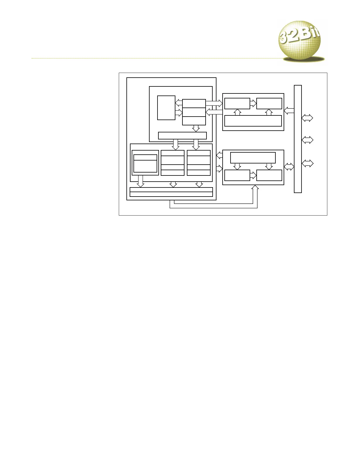
Motorola built the 680x0 archi-
tecture around 16 general regis-
ters with a 68000-compatible,
orthogonal instruction set. The
680x0 has more registers than the
original 68000. Motorola added
the control registers to control the
memory-management unit
(MMU) and the floating-point
unit (FPU) and to support addi-
tional processing capabilities. For
example, the 68040 adds eight 80-
bit floating-point registers and 12
control registers.These registers
include a vector-base register,
points to an interrupt-vector
table; a cache-control register;
user and supervisor root pointers;
and translation registers.
The superscalar 68060 heads
the 680x0 line-up with its dual
integer and floating-point pipe-
lines. As instructions enter the
CPU, they flow into a four-stage
prefetch pipeline: instruction-
address generation, instruction
cycle, instruction early decode, and instruction buffer. In this
pipeline, the 680x0 converts 68000-compatible, variable-
length CISC instructions to a fixed-length instruction. These
instructions then enter dual, four-stage, synchronously oper-
ating, integer-execution pipelines. The decode, effective-
address-calculation, fetch, and integer-execution pipeline
dispatches instructions to the FPU and allows for some exe-
cution overlap between the integer and FPU engines.
A Harvard architecture allows the 68060 to perform simul-
taneous instruction fetches and data accesses. The four-way
set-associative, four-way-interleaving, on-chip caches sup-
port simultaneous read and write operations. You can freeze
portions of the caches to prevent reallocation.
The 68040 implements a fetch, decode, effective-address-
calculation, effective-address-fetch, execute, and write-back
pipeline. To speed processing, the device has two 4-kbyte
direct-mapped caches and separate data and instruction
MMUs, which allow simultaneous address translations. The
040 includes bus snooping to ensure cache coherency for
multiprocessing. The cache supports both write-through and
copy-back modes. The 68020 and 68030 CISC implementa-
tions have smaller caches; the 030 and 040 versions imple
-
ment burst mode, moving as much as 16 bytes in an address
-
ing block between registers and memory
.
The 040 and 060 deliver apparent single-cycle execution
for some instructions, mainly register operations such as
memor
y-to-register moves if the data is in the data cache. A
taken branch takes two cycles; a not-taken branch takes
three cycles. On the 68060, a 256-entr
y, four-way
, set-asso
-
ciative, on-chip branch cache allows taken and nontaken
branches to execute in zero and one clock, respectively
. The
branch-cache unit contains state bits that provide a histor
y
of branch executions, which helps to predict branch direc
-
tion.
Unlike the 020/030, the 040 and 060 perform no dynam
-
ic bus sizing. Instead, they have a highly reliable bus with a
high-drive option that can implement a synchronous, two-
clock read/write protocol. A 4-word burst takes five clocks.
The 040 includes multiprocessor-bus arbitration but requires
off-chip logic. Externally, the 68060 bus is a superset of the
68040 bus. Additional signals support higher performance
system designs, but the processor can easily operate on a
68040-based bus. An on-chip MMU with separate instruction
and data translation-look-aside buffers allows the 68060 to
access as much as 4 Gbytes of memory.
Power management: To support power management, the
68060’s functional units respond to dynamically controlled
clocking; the caches and execution units power down when
not accessed. The static design allows you to reduce or stop
the external clock, and a low-power-stop (LPSTOP) instruc-
tion disconnects most of the chip from the clock pin.
Special instr
uctions:
The CPUs have special instructions for
variable-length bit fields; moving 16 registers; compare; and
swap, which locks memor
y for multiprocessing. A scaling
option addresses data by item size for table-access, FPU, and
MMU commands.
The 68040 and 68060 have a special move instruction
(MOVE16) to perform a 16-byte block move and a PLP
A
instruction that loads a physical address by translating a log-
ical address. A table instruction performs a table look-up and
interpolates the data.
Special peripherals: The MC68150 allows the 68040,
LC040, and EC040 bus to communicate bidirectionally with
32-, 16-, or 8-bit peripherals and memories. The XC68HC901
multifunction peripheral comprises a one-channel USART
and an eight-sour
ce interrupt controller.
Development tools: The 680x0 shares many of the same
tools as the 68EC000.
Second sources:T
oshiba acts as a second source for some ver
-
sions of the 680x0.
Motorola 680x0