158 b EDN S
EPTEMBER 24, 1998
NEC’s V800 Series mCs are available as cores
and standard products. All core versions
contain the same peripherals as those in
the standard devices. The company based
the V800, including the V830 and V850,
on a proprietary, 32-bit RISC architecture.
NEC designed the V830 for embedded mul-
timedia applications with external-memo-
ry support; the family provides on-chip
instruction and data caches with demulti-
plexed address and data buses. The V850 is
a mC with integrated RAM, ROM, and flash
options.
The V800 ar
chitecture comprises a five-
stage pipeline: fetch, decode, execute,
memory access, and write back; 32 general-
purpose registers; a 32-bit barrel shifter;
and a hardware multiplier. Most instruc-
tions execute in one clock and are 2 bytes
long, allowing smaller code. The CPU has a
pipeline-stall feature that automatically
inserts a bubble in the pipeline to avoid
data dependencies and hazards. Instruc-
tion and data accesses occur on separate
buses. Interrupt latency from an external
source or peripherals is a minimum of 11
CPU cycles.
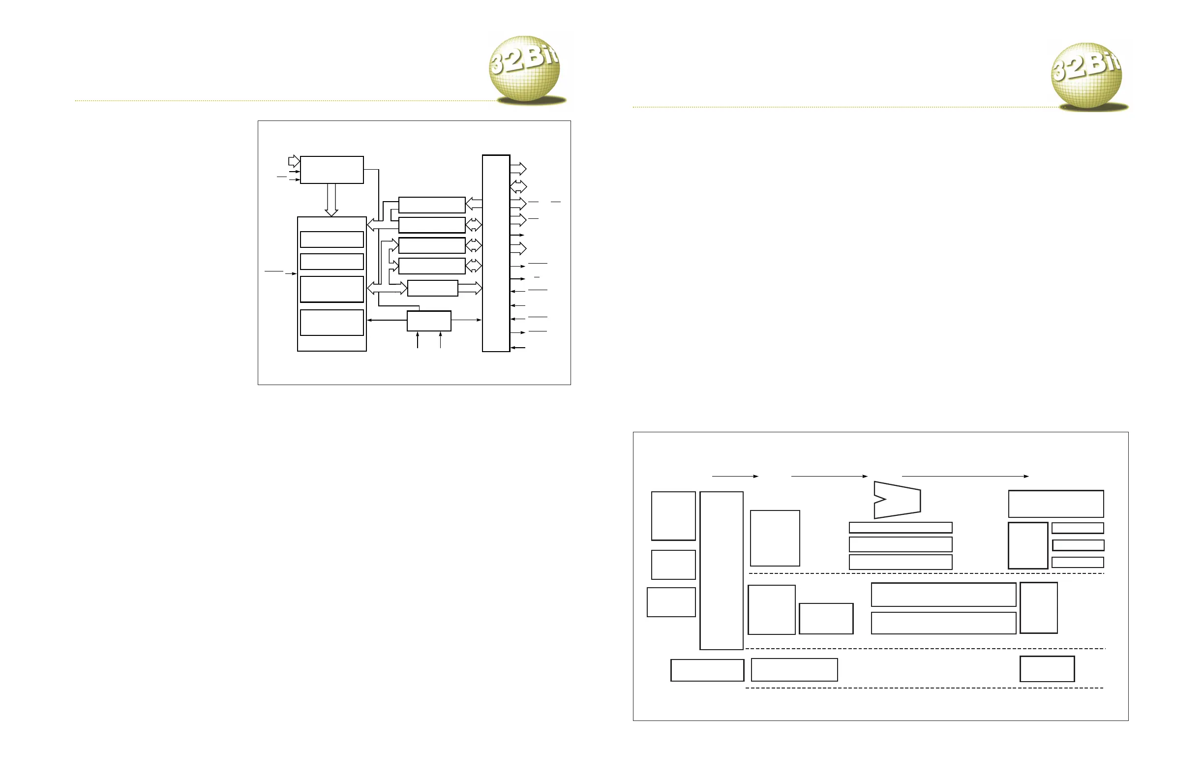
A bus-control unit (BCU) generates a
prefetch address to prefetch an instruction code from exter-
nal memory and store it in the 4-double-word prefetch
queue. For accesses from internal ROM, instructions go
straight to the CPU; that is, not through the prefetch queue.
Instruction fetches from internal ROM consume one cycle;
data fetches from ROM require three cycles. Therefore, you
should shadow look-up tables and fixed data structures to the
CPU’s internal RAM, in which the V800 can access data in
one clock. The BCU also provides a bus-arbitration function,
allowing other devices, such as DMA, to share and take con-
trol of the V851’s external bus. Programmable wait- and idle-
state insertion control facilitates interfacing to slow memory
.
Although most of the microcontrollers provide as much as 16
Mbytes (24 address bits) of linear addressing, the new V850E
also provides dynamic bus sizing. The maximum addressing
range of the V800 architecture is 4 Gbytes.
The V800 accesses peripherals as memor
y-mapped I/O that
connects to the CPU through a 16-bit bus. ROM and RAM
communicate to the CPU using a 32-bit bus. Although the
first member of this family
, the V851, has 32 kbytes of ROM
and 1 kbyte of RAM, the V850 ar
chitecture allows internal
expansion to 1 Mbyte of ROM and 4 kbytes of RAM. Similar-
ly
, the external bus of the V851 addresses as much as 16
Mbytes. (The ar
chitecture allows access to as much as 4
Gbytes on future chips.) The V850’
s memory space divides
into 1-Mbyte unit blocks, and you can insert wait states in a
bus cycle for ever
y two blocks.
Power management: In halt mode, the clock generator con
-
tinues to operate, but the CPU clock stops, allowing the on-
chip peripherals to function. Idle mode stops the CPU clock
and internal-system clock; however
, because the clock gen-
erator continues to run, normal operation can resume with
-
out waiting for oscillator and PLL stabilization. In stop mode,
everything stops, but register and memory contents stay
intact.
Special instructions:NEC’s V800 devices support a software-
trap instruction. The CPUs also perform saturate operations
in which the devices store maximum values of additions that
result in overflow. For example, if the result exceeds the pos-
itive-value 7FFFFFFFh, the CPU stores 7FFFFFFFh in the result
registers and then sets the saturation flag. The V850E device
also provides single-cycle byte-swapping operations for endi-
an translation of data structures. Also, NEC includes single
instructions to assist in C procedure calls for pushing and
popping multiple registers. The net effect would be a decrease
of code in the prologue and epilogue sections in C and a
resulting speed increase.
Special on-chip peripherals: An on-chip DRAM controller
,
synchronous flash controller, and DMA controllers are avail
-
able in the latest devices.
Development tools: NEC, Green Hills Software (www
.
ghs.com), and Cygnus Support (www.cygnus.com) offer C-
compiler tool chains for the V800. Accelerated T
echnology
(www
.atinucleus.com), Green Hills Software, NEC, JMI Soft-
ware (www.jmi.com), and W
ind River Systems (www
.win-
driver
.com) provide RTOSs. A host of stand-alone evaluation
boards, PC ISA-bus evaluation boards, and in-cir
cuit emula-
tors is available from NEC and third-party vendors. NEC
works jointly with Synopsys (www
.synopsys.com) and Men-
tor (www
.mentor.com) to provide simulation tools for the
V800 Series embedded core/ASIC development. NEC’
s Open-
CAD environment supports these tools and is compatible
with the standard device-development tools.
Second sources: There are no second sour
ces for the V800,
but Lucent T
echnologies (www.lucent.com) licenses the
V850 as a core within its cell-based ASCI librar
y.
NEC V800
EDN S
EPTEMBER
24, 1998
b 159
The Siemens Tricore architecture represents the industry’s
trend toward a blurring of the distinction between micro-
controllers and DSPs (see “Microprocessor and DSP tech-
nologies unite for embedded applications,” EDN, March 2,
1998, pg 73). This architecture’s functional units and its uni-
fied instruction set target microcontroller- and DSP-specific
functionality. Tricore is a superscalar core with two primary
four-stage pipelines; the first bit of every instruction identi-
fies which pipeline that instruction follows. One pipeline
does loops, loads, and address-generation arithmetic; the
other pipeline does all the math and branches. The execute
unit comprises a multiply-accumulate (MAC) module, an
ALU, and a tightly coupled coprocessor interface. A third
pipeline performs loop control for zero-overhead looping.
Tricore supports a mixture of 16- and 32-bit-wide instructions
to help conserve code space; each operation code includes a
size bit to improve the efficiency of instruction decoding.
Tricore implements a Harvard architecture with separate
address and data buses for program and data memories. Tri-
core is also a load/store architecture with 16 32-bit general-
purpose data registers and 16 32-bit address registers. You can
concatenate consecutive even-odd data registers to form
eight 64-bit registers for extended precision.
Unlike traditional DSPs, Tricore lacks separate X- and Y-
memory spaces, which may require you to perform some
loop unrolling to achieve the parallel performance of DSPs.
As long as data is available for Tricore’s execute unit. The
device can perform single-cycle MACs. The data side of the
core has a 128-bit-wide bus to on-chip DRAM, which you can
use to save two data and two address registers in one cycle to
the cache. Tricore supports circular buffers for DSP filters and
bit-reversed indexing for FFTs. You must align the start of the
circular buffer to a multiple of the data size, which the
instruction using the buffer prescribes. The length of the
buffer must also be a multiple of the data size the instruction
using the buffer references.
Special instructions:The instruction set supports operations
on Booleans, bit strings, characters, signed fractions, address-
es, signed and unsigned integers, single-instruction multiple-
data, and single-precision floating-point numbers. In addi-
tion to a plethora of microcontroller-oriented instructions,
such as bit manipulation, Tricore supports the traditional DSP
instructions, including multiply and MAC, saturate, scaling,
and rounding. Tricore also supports packed arithmetic. Con-
ditional add, subtract, and select instructions let the device
avoid using conditional jumps.
Development tools: Tasking (www.tasking.com) and Green
Hills Software (www.ghs.com) offer C- and C++-compiler,
debugger, simulator, and RTOS support for Tricore. Acceler-
ated Technology (www.atinucleus.com) also supplies a Tri-
core RTOS. Nohau (www.nohau.com), Ashling (www.
ashling.com), Hitex (www.hitex.de), and Lauterbach (www.
lauterbach.com) supply Tricore in-circuit emulators. Task-
ing’s instruction-accurate simulator allows you to analyze the
basic functionality of your program. Siemens also has a cycle-
accurate simulator that implements a flexible cache model
that provides options, such as defining start and end address-
es, the number of ways and cache lines, and the line size and
banks. This simulator also includes branch-prediction logic
and determines interrupt latency.
Second sources: There are no second sources for the Tricore.
Siemens Tricore