3/24/97 3-4 XA Memory Organization
Bit Access to Registers
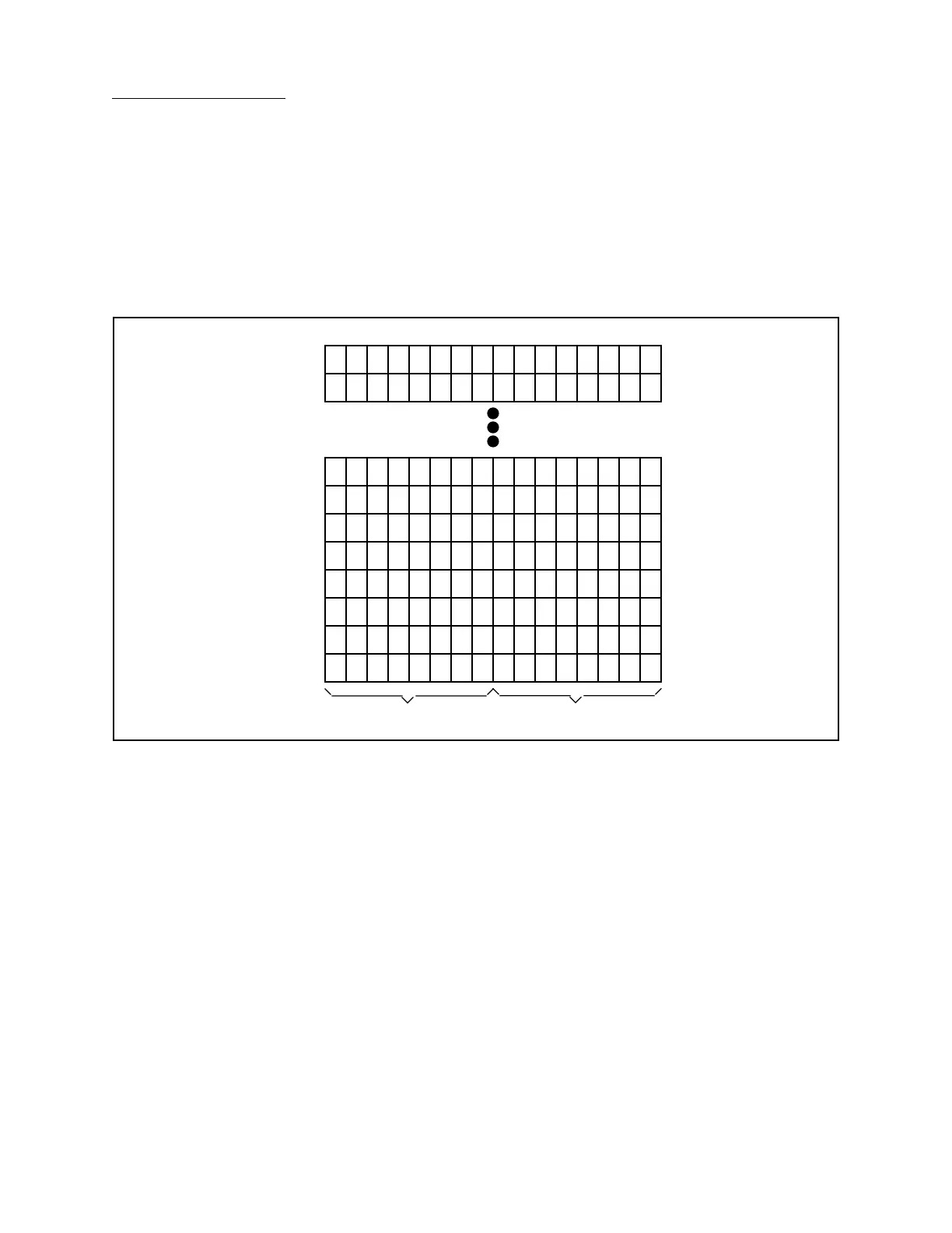
The XA Registers are all bit addressable. Figure 3.3 shows how bit addresses overlie the basic
register file map. In general, absolute bit references as given in this map are unnecessary. XA
software development tools provide symbolic access to bits in registers. For example, bit 7 may
be designated as “R0.7” with no ambiguity
Bit references to banked registers R0 through R3 access the currently accessible register bank, as
set by PSW bits RS1, RS0 and the currently selected stack pointer USP or SSP. The unselected
registers are inaccessible..
3.3 The XA Memory Spaces
The XA divides physical memory into program and data memory spaces. Twenty-four address
bits, corresponding to a 16MB address space, are defined in the XA architecture. In any given
XA implementation, fewer than all twenty-four address bits may actually be used, and there is
provision for a small-memory mode which uses only 16-bit addresses; see Chapter 4.
Code and data memory may be on-chip or external, depending on the XA variant and the user
implementation. Whether a specific region is on-chip or external does not, in general, affect
access to the memory.
Figure 3.3 Bit Address to Registers
0F 0E 0D 0C 0B 0A 09 08 07 06 05 04 03 02 01 00
R0
1F 1E 1D 1C 1B 1A 19 18 17 16 15 14 13 12 11 10
R1
R2
R3
R4
R5
R6
R14
R15
2F 2E 2D 2C 2B 2A 29 28 27 26 25 24 23 22 21 20
3F 3E 3D 3C 3B 3A 39 38 37 36 35 34 33 32 31 30
4F 4E 4D 4C 4B 4A 49 48 47 46 45 44 43 42 41 40
5F 5E 5D 5C 5B 5A 59 58 57 56 55 54 53 52 51 50
R7
6F 6E 6D 6C 6B 6A 69 68 67 66 65 64 63 62 61 60
7F 7E 7D 7C 7B 7A 79 78 77 76 75 74 73 72 71 70
EF EE ED EC EB EA E9 E8 E7 E6 E5 E4 E3 E2 E1 E0
FF FE FD FC FB FA F9 F8 F7 F6 F5 F4 F3 F2 F1 F0
RnH
RnL