XA User Guide 7-18 4/17/98
The third (and final) pullup is referred to as the "strong" pullup. This pullup is included to speed
up low-to-high transitions on a port pin when the port latch changes from 0 to 1. When this
occurs, the strong pullup turns on for a brief time, two CPU clocks, pulling the port pin high
quickly, then turning off again.
The quasi-bidirectional output structure normally provides a means to have mixed inputs and
outputs on port pins without the need for special configurations. However, it has several
drawbacks that can be problems in certain situations. For one thing, quasi-bidirectional outputs
have a very small source current and are therefore not well suited to driving certain types of
loads. They are especially unsuited to directly drive the bases of external NPN transistors, a
common method of boosting the current of I/O pins.
Also, since the weak pullup turns off when a port pin is actually low, and the strong pullup turns
on only for a brief time, it is possible that under certain port loading conditions, the port pin will
get "stuck" low and cannot be driven high. This tends to happen when an external device being
driven by the port pin has some leakage to ground that is larger than the current supplied by the
very weak pullup of the quasi-bidirectional port output. If there is also a fairly large capacitance
on the pin, from a combination of the wiring itself and the pin capacitance of the device(s)
connected to the pin, the strong pullup may not succeed in pulling the pin high enough while it is
turned on. When the strong pullup is then turned off, the leakage of the external device pulls the
pin low again, since only the very weak pullup is turned on at that point and the leakage is
greater than the very weak pullup source current. These issues are the reason for enhancing the
port configurations of the XA.
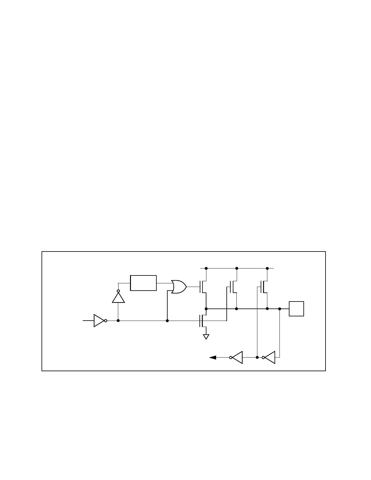
A diagram of the quasi-bidirectional output structure is shown in the figure below.
Figure 7.15 Structure of the Quasi-Bidirectional Output Configuration
weak
very
weak
strong
port
pin
Vdd
2 clock
delay
input
data
port latch
data
N
P
P
P