17
Absolute Maximum Ratings T
A
= 25
o
C Thermal Information
Supply Voltage . . . . . . . . . . . . . . . . . . . . . . . . . . . . . . . . . . . . .+8.0V
Input, Output or I/O Voltage . . . . . . . . . . . . GND-0.5V to V
CC
+0.5V
ESD Classification . . . . . . . . . . . . . . . . . . . . . . . . . . . . . . . . Class 1
Operating Conditions
Voltage Range . . . . . . . . . . . . . . . . . . . . . . . . . . . . . . +4.5V to 5.5V
Operating Temperature Range
C82C55A . . . . . . . . . . . . . . . . . . . . . . . . . . . . . . . . . .0
o
C to 70
o
C
I82C55A . . . . . . . . . . . . . . . . . . . . . . . . . . . . . . . . . -40
o
C to 85
o
C
M82C55A . . . . . . . . . . . . . . . . . . . . . . . . . . . . . . . -55
o
C to 125
o
C
Thermal Resistance (Typical, Note 1) θ
JA
θ
JC
CERDIP Package . . . . . . . . . . . . . . . . 50
o
C/W 10
o
C/W
CLCC Package . . . . . . . . . . . . . . . . . . 65
o
C/W 14
o
C/W
PDIP Package . . . . . . . . . . . . . . . . . . . 50
o
C/W N/A
PLCC Package . . . . . . . . . . . . . . . . . . 46
o
C/W N/A
Maximum Storage Temperature Range . . . . . . . . . .-65
o
C to 150
o
C
Maximum Junction Temperature
CDIP Package . . . . . . . . . . . . . . . . . . . . . . . . . . . . . . . . . . . 175
o
C
PDIP Package . . . . . . . . . . . . . . . . . . . . . . . . . . . . . . . . . . . 150
o
C
Maximum Lead Temperature (Soldering 10s) . . . . . . . . . . . . . 300
o
C
(PLCC Lead Tips Only)
Die Characteristics
Gate Count . . . . . . . . . . . . . . . . . . . . . . . . . . . . . . . . . . . 1000 Gates
CAUTION: Stresses above those listed in “Absolute Maximum Ratings” may cause permanent damage to the device. This is a stress only rating and operation
of the device at these or any other conditions above those indicated in the operational sections of this specification is not implied.
NOTE:
1. θ
JA
is measured with the component mounted on an evaluation PC board in free air.
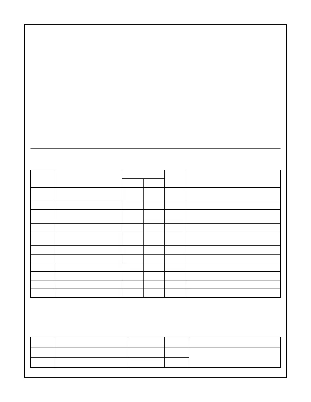
Electrical Specifications V
CC
= 5.0V ±10%; T
A
= 0
o
C to +70
o
C (C82C55A);
T
A
= -40
o
C to +85
o
C (I82C55A);
T
A
= -55
o
C to +125
o
C (M82C55A)
SYMBOL PARAMETER
LIMITS
UNITS TEST CONDITIONSMIN MAX
V
IH
Logical One Input Voltage 2.0
2.2
- V I82C55A, C82C55A,
M82C55A
V
IL
Logical Zero Input Voltage - 0.8 V
V
OH
Logical One Output Voltage 3.0
V
CC
-0.4
-VI
OH
= -2.5mA,
I
OH
= -100µA
V
OL
Logical Zero Output Voltage - 0.4 V I
OL
+2.5mA
I
I
Input Leakage Current -1.0 +1.0 µAV
IN
= V
CC
or GND,
DIP Pins: 5, 6, 8, 9, 35, 36
IO I/O Pin Leakage Current -10 +10 µA VO = V
CC
or GND DIP Pins: 27 - 34
IBHH Bus Hold High Current -50 -400 µA VO = 3.0V. Ports A, B, C
IBHL Bus Hold Low Current 50 400 µA VO = 1.0V. Port A ONLY
IDAR Darlington Drive Current -2.5 Note 2, 4 mA Ports A, B, C. Test Condition 3
ICCSB Standby Power Supply Current - 10 µAV
CC
= 5.5V, V
IN
= V
CC
or GND. Output Open
ICCOP Operating Power Supply Current - 1 mA/MHz T
A
= +25
o
C, V
CC
= 5.0V, Typical (See Note 3)
NOTES:
2. No internal current limiting exists on Port Outputs. A resistor must be added externally to limit the current.
3. ICCOP = 1mA/MHz of Peripheral Read/Write cycle time. (Example: 1.0µs I/O Read/Write cycle time = 1mA).
4. Tested as V
OH
at -2.5mA.
Capacitance T
A
= 25
o
C
SYMBOL PARAMETER TYPICAL UNITS TEST CONDITIONS
CIN Input Capacitance 10 pF FREQ = 1MHz, All Measurements are
referenced to device GND
CI/O I/O Capacitance 20 pF
82C55A