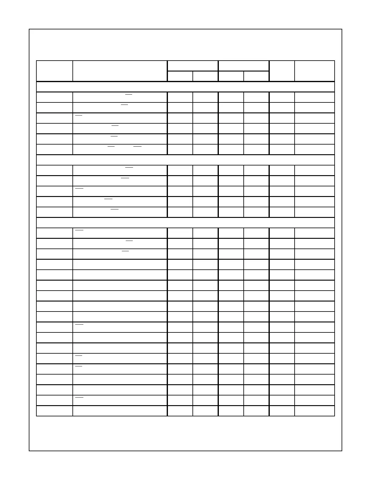
18
AC Electrical Specifications V
CC
= +5V± 10%, GND = 0V; T
A
= -55
o
C to +125
o
C (M82C55A) (M82C55A-5);
T
A
= -40
o
C to +85
o
C (I82C55A) (I82C55A-5);
T
A
= 0
o
C to +70
o
C (C82C55A) (C82C55A-5)
SYMBOL PARAMETER
82C55A-5 82C55A
UNITS
TEST
CONDITIONSMIN MAX MIN MAX
READ TIMING
(1) tAR Address Stable Before
RD 0-0-ns
(2) tRA Address Stable After
RD 0-0-ns
(3) tRR
RD Pulse Width 250 - 150 - ns
(4) tRD Data Valid From
RD - 200 - 120 ns 1
(5) tDF Data Float After
RD 10 75 10 75 ns 2
(6) tRV Time Between
RDs and/or WRs 300 - 300 - ns
WRITE TIMING
(7) tAW Address Stable Before
WR 0-0-ns
(8) tWA Address Stable After
WR 20 - 20 - ns
(9) tWW
WR Pulse Width 100 - 100 - ns
(10) tDW Data Valid to
WR High 100 - 100 - ns
(11) tWD Data Valid After
WR High 30 - 30 - ns
OTHER TIMING
(12) tWB
WR = 1 to Output - 350 - 350 ns 1
(13) tIR Peripheral Data Before
RD 0-0-ns
(14) tHR Peripheral Data After
RD 0-0-ns
(15) tAK ACK Pulse Width 200 - 200 - ns
(16) tST STB Pulse Width 100 - 100 - ns
(17) tPS Peripheral Data Before STB High 20 - 20 - ns
(18) tPH Peripheral Data After STB High 50 - 50 - ns
(19) tAD ACK = 0 to Output - 175 - 175 ns 1
(20) tKD ACK = 1 to Output Float 20 250 20 250 ns 2
(21) tWOB
WR = 1 to OBF = 0 - 150 - 150 ns 1
(22) tAOB ACK = 0 to OBF = 1 - 150 - 150 ns 1
(23) tSIB STB = 0 to IBF = 1 - 150 - 150 ns 1
(24) tRIB
RD = 1 to IBF = 0 - 150 - 150 ns 1
(25) tRIT
RD = 0 to INTR = 0 - 200 - 200 ns 1
(26) tSIT STB = 1 to INTR = 1 - 150 - 150 ns 1
(27) tAIT ACK = 1 to INTR = 1 - 150 - 150 ns 1
(28) tWIT
WR = 0 to INTR = 0 - 200 - 200 ns 1
(29) tRES Reset Pulse Width 500 - 500 - ns 1, (Note)
NOTE: Period of initial Reset pulse after power-on must be at least 50µsec. Subsequent Reset pulses may be 500ns minimum.
82C55A