Philips Semiconductors Linear Products Product specification
DAC08 Series8-Bit high-speed multiplying D/A converter
August 31, 1994
718
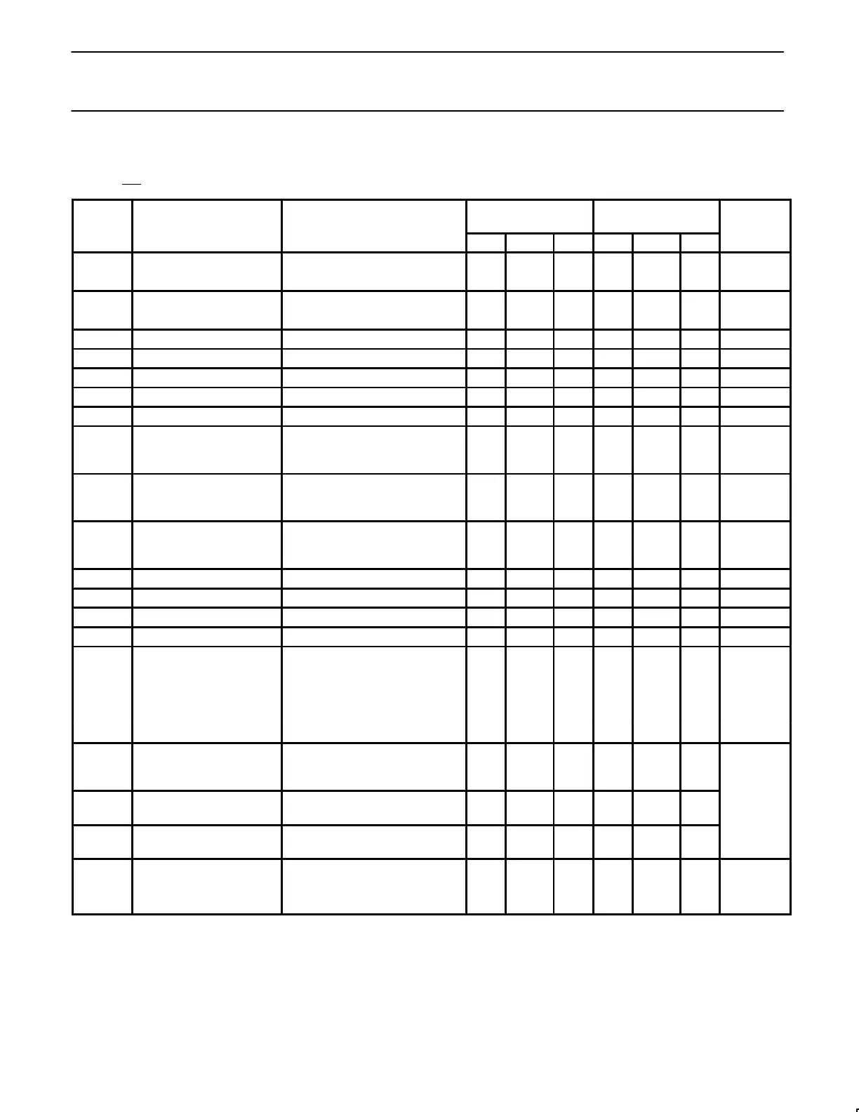
DC ELECTRICAL CHARACTERISTICS
Pin 3 must be at least 3V more negative than the potential to which R
15
is returned. V
CC
=±15V, I
REF
=2.0mA. Output characteristics refer to both
I
OUT
and I
OUT
unless otherwise noted. DAC08C, E, H: T
A
=0°C to 70°C DAC08/08A: T
A
=-55°C to 125°C
Resolution 8 8 8 8 8 8 Bits
Monotonicity 8 8 8 8 8 8 Bits
Relative accuracy Over temperature range ±0.39 ±0.19 %FS
Differential non-linearity ±0.78 ±0.39 %FS
TCI
FS
Full-scale tempco ±10 ±10 ppm/°C
V
OC
Output voltage compliance Full-scale current change< 1/2LSB -10 +18 -10 +18 V
I
FS4
Full-scale current V
REF
=10.000V, R
14
, R
15
=5.000kΩ 1.94 1.99 2.04 1.94 1.99 2.04 mA
I
FSS
Full-scale symmetry I
FS4
-I
FS2
±2.0 ±16 ±1.0 ±8.0 µA
I
ZS
Zero-scale current 0.2 4.0 0.2 2.0 µA
I
FSR
Full-scale output current
range
R
14
, R
15
=5.000kΩ
V
REF
=+15.0V, V-=-10V
V
REF
=+25.0V, V-=-12V
2.1
4.2
2.1
4.2
mA
V
IL
V
IH
Logic input levels
Low
High
V
LC
=0V
2.0
0.8
2.0
0.8 V
I
IL
I
IH
Logic input current
Low
High
V
LC
=0V
V
IN
=-10V to +0.8V
V
IN
=2.0V to 18V
-2.0
0.002
-10
10
-2.0
0.002
-10
10
µA
V
IS
Logic input swing V-=-15V -10 +18 -10 +18 V
V
THR
Logic threshold range V
S
=±15V -10 +13.5 -10 +13.5 V
I
15
Reference bias current -1.0 -3.0 -1.0 -3.0 µA
dl/dt Reference input slew rate 4.0 8.0 4.0 8.0 mA/µs
Power supply sensitivity I
REF
=1mA
PSSI
FS+
Positive V+=4.5 to 5.5V, V-=-15V; 0.0003 0.01 0.0003 0.01
V+=13.5 to 16.5V, V-=-15V %FS/%VS
PSI
FS-
Negative V-=-4.5 to -5.5V, V+=+15V; 0.002 0.01 0.002 0.01
V-=-13.5 to -16.5, V+=+15V
I+
I-
Power supply current
Positive
Negative
V
S
=±5V, I
REF
=1.0mA
3.1
-4.3
3.8
-5.8
3.1
-4.3
3.8
-5.8
I+
I-
Positive
Negative
V
S
=+5V, -15V, I
REF
=2.0mA
3.1
-7.1
3.8
-7.8
3.1
-7.1
3.8
-7.8
mA
I+
I-
Positive
Negative
V
S
=±15V, I
REF
=2.0mA
3.2
-7.2
3.8
-7.8
3.2
-7.2
3.8
-7.8