1
http://www.intersil.com or 407-727-9207 | Copyright © Intersil Corporation 1999
Interfacing the 80C286-16 with the 80287-10
Introduction
An important requirement in many systems is the ability to
off-load numeric data processing. In an 80C286 system, this
can be accomplished with an 80287 numeric co-processor.
However, as processor speeds increase, it may become
necessary to interface a high speed 80C286 processor with
a lower speed 80287. This Document will briefly describe the
interface between a 16MHz 80C286 (80C286-16) and a
10MHz 80287 (80287-10).
Interfacing the 80C286 with an 80287 can be broken down
into three main areas:
(1) Bus control lines and data lines which coordinate and
implement the flow of data between the two processors
(i.e. the data lines, chip select lines, and read/write
lines).
(2) The clock line(s), which drive the two processors.
(3) The four status lines through which the 80C286 and
80287 directly communicate status information to one
another - comprised of the
BUSY, ERROR, Peripheral
Request (PEREQ), and Peripheral Acknowledge
(
PEACK) lines.
Bus Control Lines
The various bus control and data lines in most systems
would be coordinated by either a bus controller (such as the
82C288), or a bus controller subsection of an 80C286
oriented chip set. All requisite bus control timing between a
16MHz 80C286, and a 10MHz 80287 would then be handled
by these devices (typically with one wait-state inserted to
allow for the slower 80287-10).
Clock Lines
A system using a 16MHz 80C286 with a 10MHz 80287
requires separate clock lines for the two processors. The
32MHz system clock used by the 80C286-16 is too fast for
the 80287 ±10, necessitating a dedicated clock driver for the
80287. This clock driver should supply a 10MHz clock to the
80287 with a 1/3 duty cycle to allow the 80287-10 to run at
it’s full 10MHz capability. One solution for providing this clock
is the 82C84A-1, which meets this specification with either a
30MHz crystal at it’s crystal inputs, or a 30MHz external
frequency input to it’s EFl pin. In either case, a 10MHz 1/3
duty cycle clock is output to the 80287. Note that when using
a dedicated clock driver such as this, the CKM pin of the
80287 must be pulled up.
Status Lines
The 80C286 and 80287 communicate status information
with one another through four signals; the
BUSY line, the
ERROR line, the peripheral request line (PEREQ), and the
PEACK line.
The
BUSY and ERROR lines can be connected from the
80287 to a 80C286-oriented chipset, or from the 80287
directly to a 80C286. In the case of the chipset interface, the
signal timing between the 80287 and 80C286 is coordinated
by the chipset. In the case of the direct 80287 to 80C286
interface, the signal timing is handled by the 80C286, and,
since the signal flow direction is from the 80287 to the
80C286 (i.e. from the slower device to the faster device), no
additional hardware is required to achieve proper timing.
The peripheral request (PEREQ) line should be connected
directly from the 80287 to the 80C286, and again, since the
signal flow direction is from the 80287 to the 80C286, no
additional hardware is required.
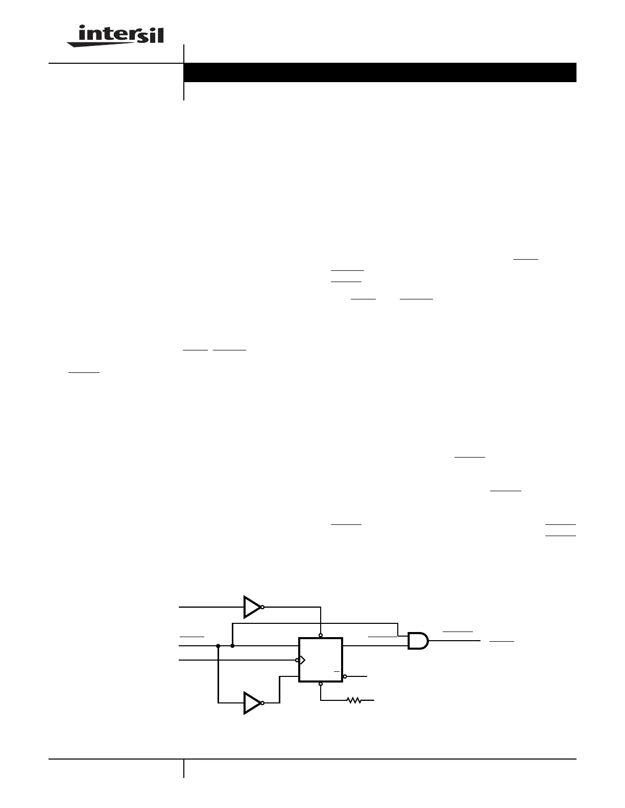
The peripheral acknowledge (
PEACK) line is normally con-
nected directly from the 80C286 to the 80287. In this case
the signal flow direction is from the 80C286 to the 80287 (i.e.
faster device to slower device), and the
PEACK active time is
not guaranteed to meet the requirements of the slower
80287-10. Worst case timing for the 80C286-16 reveals that
PEACK output could be as short as 45.5ns (i.e. PEACK
(min) = 45.5ns). The 80287-10 input requirement is
PEACK
(min) = 60ns. (min) = 45.5ns). The 80287-10 input require-
FIGURE 1. PEACK STRETCH CIRCUIT
(FROM 82C284 OR
EQUIVALENT)
RESET 1 2
U1 74AC04
3
1
2
34
U1 74AC04
PEACK
286_CLK
(FROM 80C286)
(32MHz SYSTEM
CLOCK)
J
C
K
PR
Q
Q
4
1
5
R1 10K
+5V
6
5
U2 74AC112
LPEACK
2
1
U3 74AC08
GPEACK
(TO 80287
PEACK)
3
Application Note March 1997 AN120.1