2
All Intersil semiconductor products are manufactured, assembled and tested under ISO9000 quality systems certification.
Intersil semiconductor products are sold by description only. Intersil Corporation reserves the right to make changes in circuit design and/or specifications at any time with-
out notice. Accordingly, the reader is cautioned to verify that data sheets are current before placing orders. Information furnished by Intersil is believed to be accurate and
reliable. However, no responsibility is assumed by Intersil or its subsidiaries for its use; nor for any infringements of patents or other rights of third parties which may result
from its use. No license is granted by implication or otherwise under any patent or patent rights of Intersil or its subsidiaries.
For information regarding Intersil Corporation and its products, see web site http://www.intersil.com
Sales Office Headquarters
NORTH AMERICA
Intersil Corporation
P. O. Box 883, Mail Stop 53-204
Melbourne, FL 32902
TEL: (407) 724-7000
FAX: (407) 724-7240
EUROPE
Intersil SA
Mercure Center
100, Rue de la Fusee
1130 Brussels, Belgium
TEL: (32) 2.724.2111
FAX: (32) 2.724.22.05
ASIA
Intersil (Taiwan) Ltd.
7F-6, No. 101 Fu Hsing North Road
Taipei, Taiwan
Republic of China
TEL: (886) 2 2716 9310
FAX: (886) 2 2715 3029
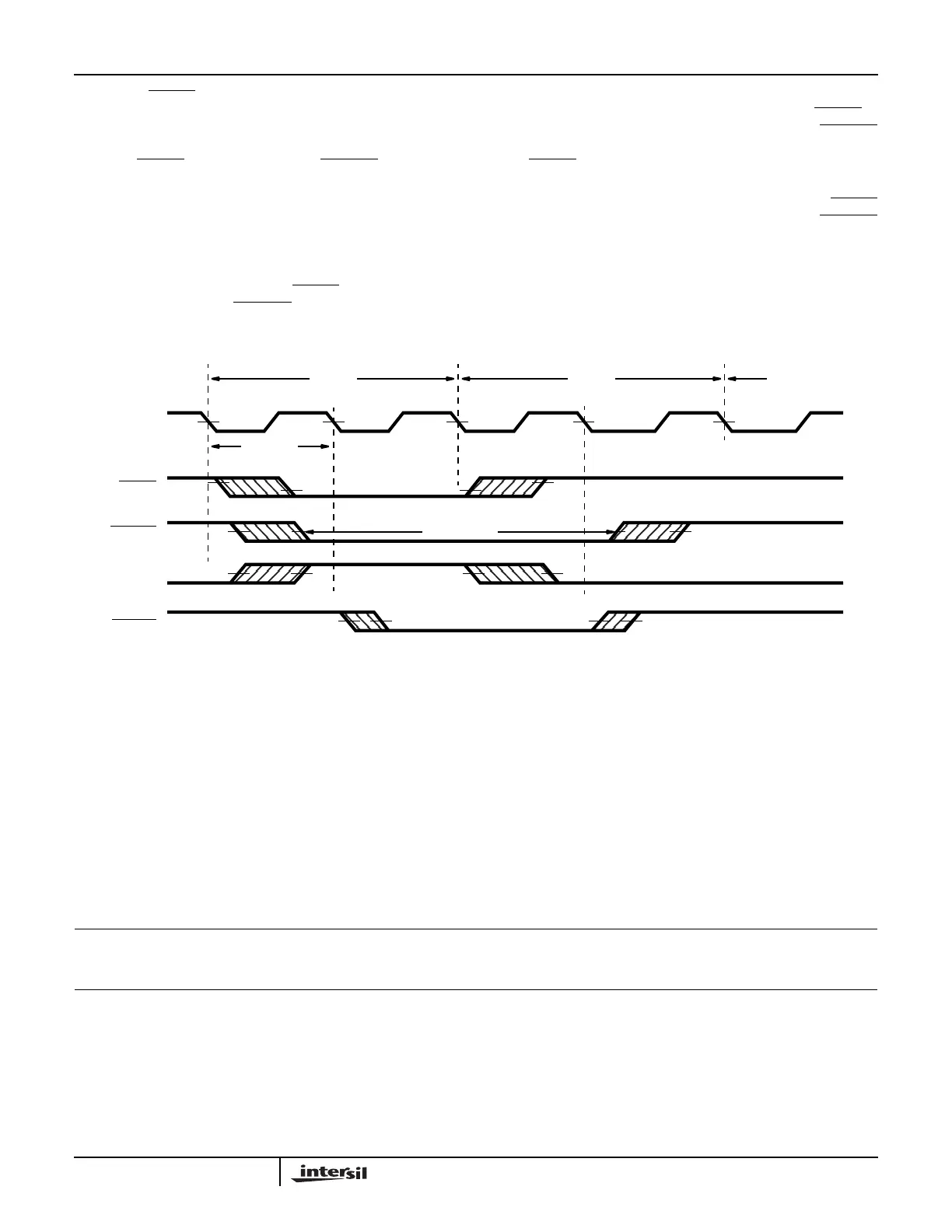
The proper PEACK timing can be achieved using the circuit
shown in Figure 1 comprised of a 74AC04, 74AC08, and a
74AC112. Referring to the timing diagram shown in Figure 2,
it can be seen that this circuit effectively “stretches” the
80C286’s
PEACK output (in the form of GPEACK) to 72.7ns,
which satisfies the 80287-10 requirement.
The operation of the circuit shown in Figure 1 is as follows:
(1) The RESET signal (which is also applied to the 80C286)
is used to initialize the ‘AC112 to a known inactive state
(Q = 1).
(2) When the 80C286 asserts the PEACK signal, the gated
version of this signal (
GPEACK) is asserted with minimal
delay (7.9ns through the ‘AC08).
(3) On the falling edge of the 80C286 CLK at the beginning
of Phase 2 of the T
S
cycle, the low state of PEACK is
clocked into the ‘AC112. This effectively holds
GPEACK
low for an additional clock cycle longer than standard
PEACK timing.
(4) On the falling edge of the 80C286 CLK at the beginning
of phase 2 of the first T
C
cycle, the high state of PEACK
is clocked into the ‘AC112, which then causes
GPEACK
to go inactive.
The net effect of this circuit operation is to extend the
80C286’s Peripheral Acknowledge signal to the 80287-10
sufficiently to meet it’s requirements.
FIGURE 2. PEACK CYCLE TIMING
φ1 φ2 φ1 φ2
T
C
T
C (WAIT)
T
S
80C286
CLK
PEACK
GPEACK
PEACK
AT K
LPEACK
31.2ns
(32MHz)
118
3.2 25.9
2.7 23.9
2.7 9.4 2.7 9.4
120
4.9 17.3
72.7ns (MIN)
2.7 25.9
Application Note 120