12713020-002-2 Revision D – April 2004 SSU-2000 User’s Guide 13
Figures
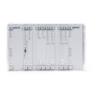
1-1 SSU-2000 Synchronization Supply Unit . . . . . . . . . . . . . . . . . . . . . . . . . 26
1-2 SSU-2000 Configured as a TSG. . . . . . . . . . . . . . . . . . . . . . . . . . . . . . . 27
1-3 SSU-2000 Configured as a Primary Reference Source . . . . . . . . . . . . . 28
1-4 SSU-2000 Configured as a Monitor-Only System. . . . . . . . . . . . . . . . . . 28
1-5 Block Diagram of the SSU-2000 . . . . . . . . . . . . . . . . . . . . . . . . . . . . . . . 29
1-6 Components in a Typical SSU-2000 Installation . . . . . . . . . . . . . . . . . . . 37
1-7 Slot Numbering Assignments . . . . . . . . . . . . . . . . . . . . . . . . . . . . . . . . . 38
1-8 Rear Panel of the SSU-2000 Main Shelf. . . . . . . . . . . . . . . . . . . . . . . . . 39
1-9 Location of Power Fuses on the Rear Panel. . . . . . . . . . . . . . . . . . . . . . 41
1-10 SSU-2000 Input/Output Connectors . . . . . . . . . . . . . . . . . . . . . . . . . . . . 47
1-11 I/O Adapter Panels for Input and Output Modules. . . . . . . . . . . . . . . . . . 48
1-12 Front View of the SDU-2000 Expansion Shelf. . . . . . . . . . . . . . . . . . . . . 53
1-13 Rear VIew of the SDU-2000 Expansion Shelf. . . . . . . . . . . . . . . . . . . . . 53
1-14 SDU-2000 Block Diagram . . . . . . . . . . . . . . . . . . . . . . . . . . . . . . . . . . . . 55
2-1 Shelf and I/O Adapter Rack Mounting. . . . . . . . . . . . . . . . . . . . . . . . . . . 63
2-2 Frame and Logic Ground Jumpers . . . . . . . . . . . . . . . . . . . . . . . . . . . . . 65
2-3 Power Terminal Blocks . . . . . . . . . . . . . . . . . . . . . . . . . . . . . . . . . . . . . . 66
2-4 SSU-2000 Rear Panel. . . . . . . . . . . . . . . . . . . . . . . . . . . . . . . . . . . . . . . 67
2-5 Installing the Output Summer Adapter . . . . . . . . . . . . . . . . . . . . . . . . . . 68
2-6 DPDT Slide Switch . . . . . . . . . . . . . . . . . . . . . . . . . . . . . . . . . . . . . . . . . 70
2-7 Alarm Terminal Blocks. . . . . . . . . . . . . . . . . . . . . . . . . . . . . . . . . . . . . . . 71
2-8 SDU Interface (J8) and Backup Clock (J9) Connectors . . . . . . . . . . . . . 74
2-9 SDU Interface (J17 and J15) and Backup Clock (J16) Connectors . . . . 74
2-10 SSU Interface (J8) Expansion Terminator . . . . . . . . . . . . . . . . . . . . . . . . 75
2-11 Wiring Diagram for a Single SDU-2000 Shelf . . . . . . . . . . . . . . . . . . . . . 76
2-12 Wiring Diagram for Multiple SDU-2000 Shelves . . . . . . . . . . . . . . . . . . . 78
2-13 SSU-2000 Power Fuses . . . . . . . . . . . . . . . . . . . . . . . . . . . . . . . . . . . . . 84
3-1 Direct Connection Using the Serial Port . . . . . . . . . . . . . . . . . . . . . . . . . 89
5-1 Alarm and Event Status Breakdown . . . . . . . . . . . . . . . . . . . . . . . . . . . 117
6-1 Block Diagram of the Stratum 2E Clock Module . . . . . . . . . . . . . . . . . . 125
6-2 Front Panel of the Stratum 2E Clock Module . . . . . . . . . . . . . . . . . . . . 126
6-3 Block Diagram of the Stratum 3E Clock Module . . . . . . . . . . . . . . . . . . 129
6-4 Front Panel of the Stratum 3E Clock Module . . . . . . . . . . . . . . . . . . . . 130
6-5 Block Diagram of the Type 1 Clock Module. . . . . . . . . . . . . . . . . . . . . . 133
6-6 Front Panel of the Type 1 Clock Module . . . . . . . . . . . . . . . . . . . . . . . . 134
6-7 Block Diagram of the Communications Module. . . . . . . . . . . . . . . . . . . 137
6-8 Front Panel of the Communications Module . . . . . . . . . . . . . . . . . . . . . 138
7-1 Block Diagram of the 1-Port and 3-Port E1 Input Modules . . . . . . . . . . 145
7-2 Front Panel of the E1 Input Module. . . . . . . . . . . . . . . . . . . . . . . . . . . . 151
7-3 Block Diagram of the 1-Port and 3-Port DS1 Input Module. . . . . . . . . . 154
7-4 Front Panel of the DS1 Input Module . . . . . . . . . . . . . . . . . . . . . . . . . . 160
7-5 Block Diagram of the GPS Input Module. . . . . . . . . . . . . . . . . . . . . . . . 163
7-6 Front Panel of the GPS Input Module . . . . . . . . . . . . . . . . . . . . . . . . . . 164
7-7 Block Diagram of the Composite Clock Input Module. . . . . . . . . . . . . . 166
 Loading...