Signal Names and Definitions
414 SSU-2000 User’s Guide 12713020-002-2 Revision D – April 2004
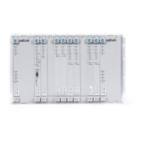
50-Pin Connector Input and Output Signals
Table D-6 corresponds the 50-pin I/O signal connectors to the appropriate I/O slot
location. The connectors J10 through J18 are hard wired through the backplane to
I/O slots A3 through A11.
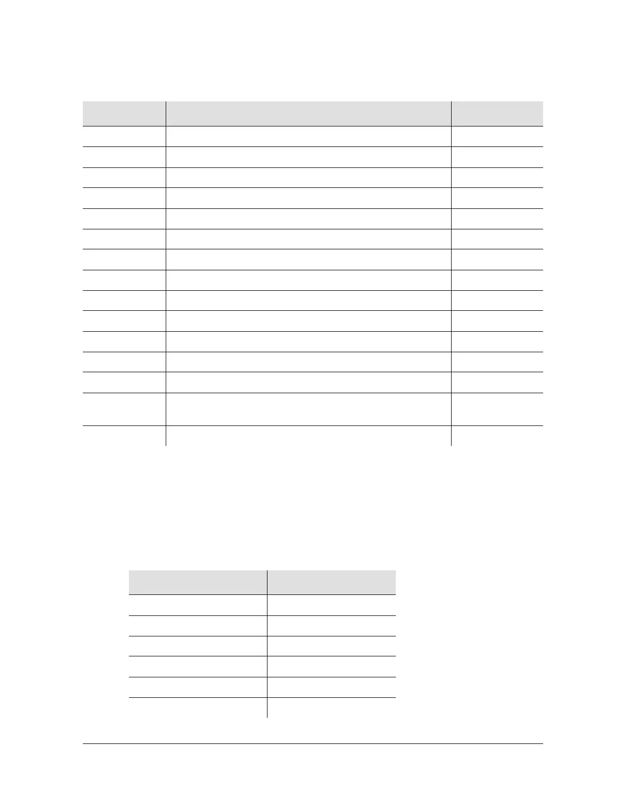
Table D-5. Signal Names and Locations for SDU-2000 Interface
Name
Description Connector–Pin
SCLK2+/– SPI Clock Signal, generated by SPI Master J8-1&14
MOSI2+/– SPI Master Out / Slave In Data line J8-2&15
MISO2+/– SPI Master In / Slave Out Data line J8-3&16
SS2+/– SPI Slave Select line, generated by SPI Master J8-5&18
SBUSY2+/– SPI Slave Busy line, generated by SPI Slave J8-4&17
SRQ2+/– SPI Service Request line, generated by SPI Slave J8-6&19
CLKAOUT2+/– Clock A to Output Modules (synced 4 kHz) J8-7&20
CLKBOUT2+/– Clock B to Output Modules (synced 4 kHz) J8-8&21
CLKC2+/– Pass-through Clock from Input to Output Modules (4 kHz) J8-9&22
CLKD2+ Selected Clock via TBNC/BNO to SDU-2000 (Backup 4 kHz) J9-A
CLKD2– Selected Clock via TBNC/BNO to SDU-2000 (Backup 4 kHz) J9-B
EXPSP1+/– Spare Connection to SDU-2000 J8-11&24
EXPSP2+/– Spare Connection to SDU-2000 J8-12&25
SOUT2+/–
SPI Expansion Shelf Select Request, generated by SDU SPI
Slave
J8-10&23
LG Logic Ground Connection J8-13
Table D-6. I/O Slot Locations
Rear Panel Connector I/O Slot Location
J10 A3
J11 A4
J12 A5
J13 A6
J14 A7
J15 A8
 Loading...