124 b EDN S
EPTEMBER 24, 1998
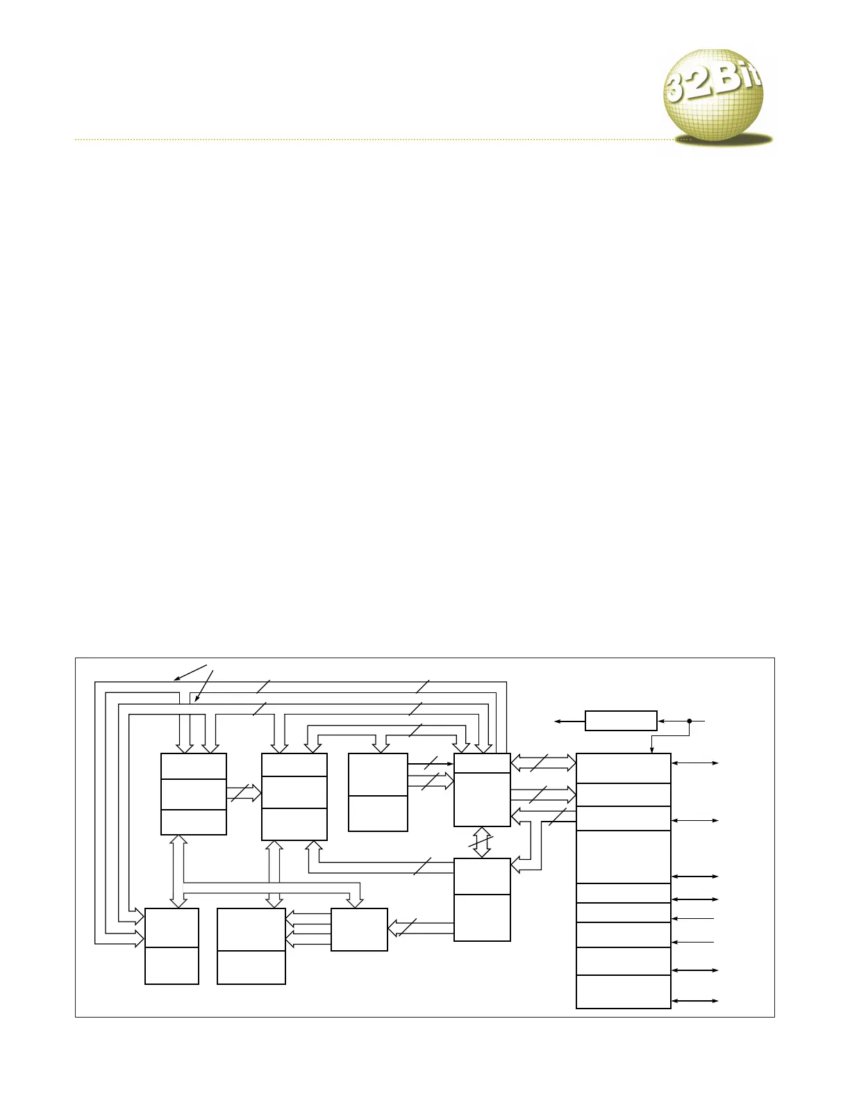
The 486 builds on the 386 architecture by adding a more effi-
cient memory bus; an on-chip floating-point unit; an on-
chip, unified, Level 1 cache; and a RISC-like implementation
for the core load/store instructions. The 32-bit 80486 imple-
mentation retains the i386’s complex instruction set but
relies on a pipelined RISC-like implementation to speed exe-
cution for simple load/store instructions. The standard 486
microarchitecture has a five-stage pipeline and uses two of
those stages, decoder stages D1 and D2, to decode the com-
plex instruction set.
The 486 chips use 1- to 15-byte-long instructions for com-
plex operations. The two decoder stages give the hardware
time to delineate and decode the instructions waiting in the
instruction queue. The instruction or byte-code queue holds
32 bytes for decoding. By fetching 4 words at a time from off-
chip or local memory, the hardware minimizes contention
between data and instruction accesses of the cache. To speed
processing, the hardware loads and writes cache lines in 4-
word bursts.
The DX4 has a unified cache that is four-way set-associa-
tive and implements a write-through policy: Writes to cache
pass through to memory, which raises memory bandwidth.
The 486’s bus and cache implement a bus-snooping protocol
for multiprocessor operation. The bus is more efficient than
that of the 386 and has a two-clock single read or write; 4-
word read bursts take five cycles and constitute most 486 bus
accesses. The processors also support secondary Level 2 cache
for both single-processor and multiprocessor operation, as
well as write-through/write-back protocols.
The 486 has four code/data breakpoint registers and two
control registers for debugging. You can set the breakpoint
registers with addresses for halting execution on a program
or data access.
Power management: The standard 486 employs system-
management mode (SMM) for power management, which
enables code to control CPU power without rewriting or
revamping operating software. The CPU enters SMM via a
hardware interrupt, the system-management interrupt (SMI);
the SMI code can set SMMs to reduce chip power dissipation.
A halt instruction powers down most of the CPU’s logic.
Special instructions: The 486 instruction set builds upon
that of the 80386, adding instructions such as byte swap,
exchange and add, compare and exchange, invalidate data
cache, write-back and invalidate data cache, invalidate trans-
lation-look-aside-buffer entry, processor identification, and
SMM resume.
Special on-chip peripherals: AMD’s ElanSC400 microcon-
troller combines an Am486 CPU with a PC/A
T chip set and
essential embedded-PC peripherals. The ElanSC400 also
includes mobile-computing peripherals, such as PLL clock
generators, PCMCIA-card support, LCD-graphics control, a
memory controller, DMA and interrupt controllers, a real-
time clock, a serial port, and a parallel port.
Development tools: Most of the tool support for the 486 is
the same as that for the 386. AMD, Intel, and National offer
evaluation kits for each of their 486 processors. For example,
AMD’s $950 mforCE (micro for CE) demonstration system for
mobile and embedded product development uses the AMD’s
ElanSC400 microcontroller and the QNX (www.qnx.com)
Realtime OS or Microsoft (www.microsoft.com) Windows CE
OS. The board contains an external matrix scan keyboard, a
flash minicard slot, a PCMCIA type 2 slot, an IrDA interface,
a serial port, a 10-bit digitizer controller for pen input, an
audio chip, and 4 Mbytes of ROM and DRAM.
Second sources: There are no pin-compatible second sources
for the 80486. AMD, Intel, and STMicroelectronics act as sec-
ond sources for some implementations.
80486