EDN S
EPTEMBER
24, 1998
b 145
144 b EDN S
EPTEMBER 24, 1998
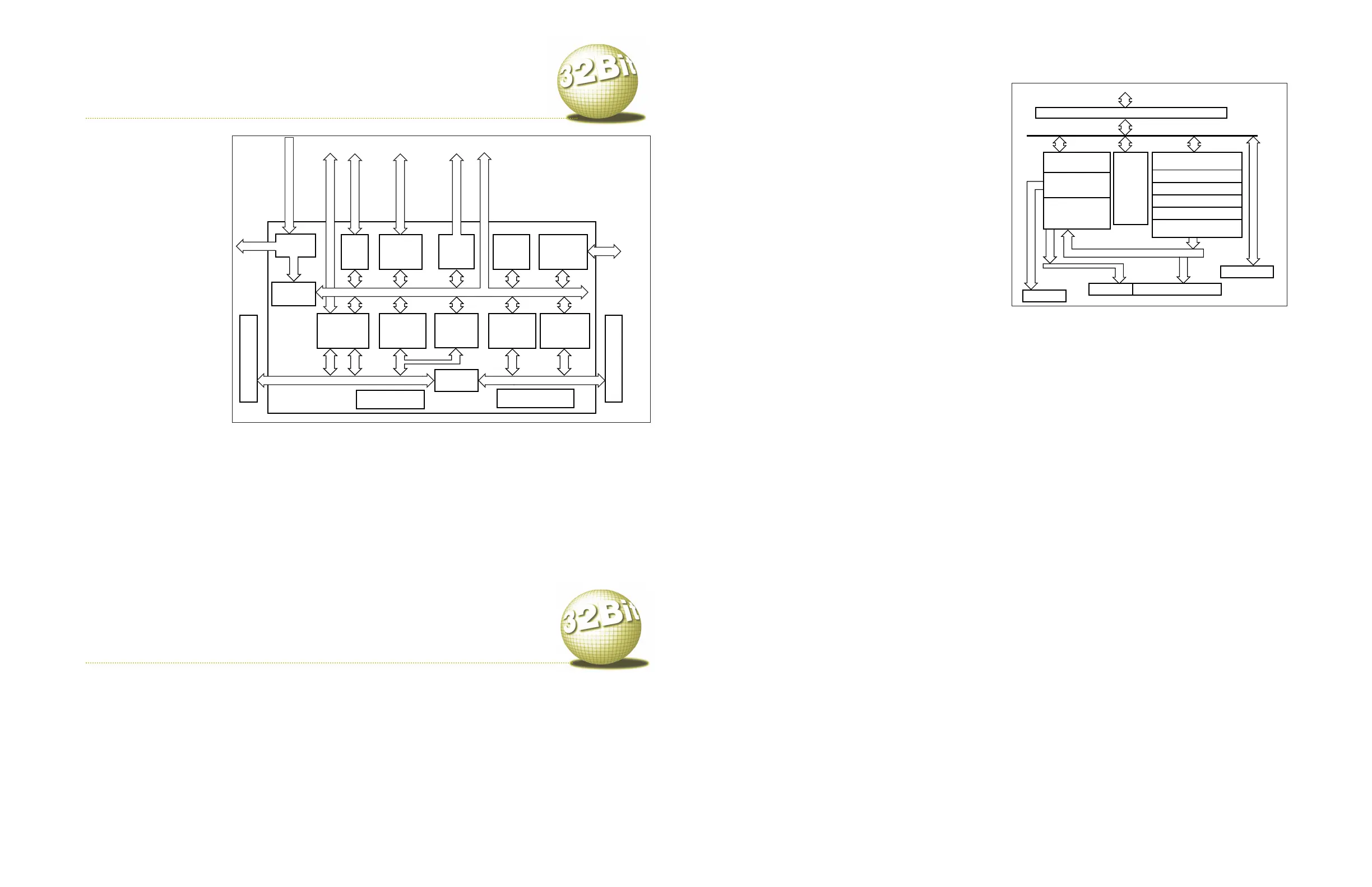
The range of i960s runs from
the new superscalar
HA/HD/HT to the 16-bit SA/SB
variants, including low-power
versions of the i960 Jx series
that operate at 3.3V. The i960
combines a von Neumann
architecture with a load/store
architecture that centers on a
core of 32 32-bit general-pur-
pose registers comprising 16
local and 16 global registers.
An on-chip register cache
automatically caches the local
register sets to speed context
switching. If the cache is full,
the oldest cached set moves to
memory, and the latest set
caches. All i960s have multi-
stage pipelines and use re-
source “scoreboarding” to
track resource usage.
The i960CA provides super-
scalar operation and five pipe-
line stages. The key to the Cx is
its four-instruction-wide in-
struction decoder, which decodes as many as four instruc-
tions per cycle. Current implementations dispatch as many
as three of these instructions for execution. The i960CF has
128-bit-wide buses to move instructions to the decoder and
128-bit-wide buses to move data between the cache and reg-
isters.
Intel built the superscalar i960s around a six-port register
file with register or memory-control execution units. These
units include an integer unit, a floating-point unit, and an
interrupt-control unit on the register side and address-gener-
ation and bus-controller units on the memory side. The i960s
can cache instructions in a lockable cache; later versions add
an instruction cache to supplement the register cache.
Intel based the i960Rx series I/O processors on the i960 Jx
series processor core. The i960Rx processors target server-
motherboard and adapter-card applications, in which the
processors create an “intelligent” I/O subsystem. Intel and
others have developed an intelligent I/O (I
2
O) specification
to speed I/O processing and simplify driver development.
Special instructions: The i960 family has uninterruptible
atomic add and modify instructions. Other instructions flush
local registers and provide cache-locking control.
Development tools: More than 70 vendors support the i960
with a robust tool suite. These vendors offer a range of com-
pilers, emulators, evaluation boards, debugging monitors,
and real-time operating systems for the i960 family.
MIPS (www
.mips.com) built the MIPS R3000 processors
around a set of 32-bit, general-purpose registers in a central
register file. T
o minimize control logic and improve speed,
the instruction set has only 73 instructions, and addressing
options are few
. The chip has a three-address load/store archi
-
tecture. Similarly
, instructions are one 32-bit word to mini-
mize decoding and speed processing. T
o reduce code size,
MIPS and LSI Logic codesigned the MIPS16 application-spe
-
cific extension. MIPS16 comprises new 16-bit instructions
with a corresponding decoding block that the MIPS mP core
integrates. Although most applications still need to run 32-
bit code (MIPS16 supports a mixture of 32- and 16-bit code),
MIPS claims that MIPS16 provides an overall memor
y savings
as large as 40%. LSI Logic, with its T
inyRISC TR4101, is the
first MIPS licensee to implement the MIPS16 instruction
extensions.
MIPS engineers implemented a five-stage pipeline: instruc
-
tion fetch, read operand and decode instruction, execute,
access data memor
y, and write back results for the R3000. The
pipeline lets as many as five instructions execute concurrent
-
ly—each at a different stage of its instruction cycle. A branch-
delay slot minimizes branch effects. The compiler fills the
instruction slot, following the branch with a no-operation
instruction or an instruction from the current thread that can
execute before the branch takes effect. T
oshiba’s R3900 and
Integrated Device T
echnology’s (IDT) RISCore32300, R3000
Intel i960
MIPS R3000
derivatives, incorporate register “scoreboarding” to enable
nonblocking loads and avoid pipeline stalls when there are
no data dependencies in subsequent instructions. This fea-
ture has a significant benefit in communications applica-
tions: It allows programmers to hide main-memory latencies
during routing or packet processing. On IDT’s 32300, you can
also use the nonblocking load for cache prefetch and for per-
forming DMA transfers without performing invalidates and
write-backs. IDT implemented this feature as a new hint,
called “ignore hint.” This feature helps you get around the
MIPS instruction-set architecture’s lack of “move-multiple”
operations. The 32300 also supports a mechanism to mini-
mize pipeline stalls; in the event of a cache miss, the first
entering word goes directly to the pipeline.
To improve the multiply and divide performance of the
standard R3000, IDT built in a dedicated integer multiply/
divide unit. In the MIPS instruction-set architecture, multi-
ply and divide use special destination registers, permitting
only one multiply at a time. IDT enhances this capability
with a three-operand multiply, whereby the operand results
go directly to a general register. This feature supports DSP
capability and performs atomic multiply adds and multiply
subtracts. It also implements count-leading ones and zeros
operations. The multiply-add throughput is one cycle faster
than the data latency, so if you use two distinct operands, the
operation becomes load-bound. Whereas the general MIPS
mechanism supports reset, cache/parity error, user transla-
tion-look-aside-buffer (TLB) miss, and general interrupts,
IDT’s 32300 lets you define separate interrupts to support
software compatibility with your legacy code.
The standard R3000 memory-management unit includes a
fully associative, 64-entry TLB that translates virtual address-
es to 32-bit physical addresses. (Note: Not all R3000 deriva-
tives contain the TLB.) The mP uses a write-through cache pol-
icy. A small on-chip FIFO buffer enables the CPU to perform
instruction “streaming”—refilling the cache and executing
instructions even while reading additional instructions from
memory.
Special instructions: The R3000 implements the MIPS-I
instruction set. IDT’s 32300 uses the MIPS II instruction-set
architecture but includes some MIPS-IV functions. It imple-
ments those MIPS-IV instructions, such as prefetch opera-
tions and conditional moves, that are independent of
operand size. The 32300 also supports both big- and little-
endian data types. Several of the MIPS derivatives add a mul-
tiply-accumulate (MAC) instruction. LSI is the first MIPS
licensee to implement MIPS16 instruction extensions on the
TinyRISC TR4101. T
oshiba’
s TX19 also uses the MIPS16
instruction extensions. (See R4xxx, pg 169, for more details.)
Special on-chip peripherals:Philips offers the T
woChipPIC,
which combines the UCB1200 that interfaces with the com-
pany’
s PR31700 MIPS
mP
. The TwoChipPIC provides a
microsystem on a chip for handheld devices. Integrated mod
-
ules include a MAC unit, an LCD controller, an infrared con
-
troller
, PCMCIA-card support, touchscreen control, and
audio in/out. T
oshiba’s peripherals include a graphics con
-
troller
, a PCI controller, and support for Microsoft’
s
(www
.microsoft.com)Windows CE.
Development tools: A range of third-party development
tools is available for the MIPS RISC ar
chitecture. Detailed
information is available in the MIPS RISC Resour
ce Catalog
from MIPS T
echnologies Inc or at www.mips.com. Philips
supplies the hardware-abstraction layer
, device drivers, a ref-
erence design, and a development board for W
indows CE
implementation on the T
woChipPIC. Microsoft’s V
isual C++
tool chain supports TwoChipPIC development.
LSI Logic offers evaluation boards and kits for its line of
TinyRISC and MiniRISC mPs and cores. For example, the com-
pany’s BDMR4101 evaluation board uses an 81-MHz TR4101
CPU core and features 1 Mbyte of SRAM and an 8-Mbyte
plug-in DRAM single-inline-memory module, 512 kbytes of
flash, a full-duplex serial port, SCN2681 dual UART with dual
RS-232C ports, the DP83934 Sonic Ethernet controller with a
10BaseT interface, and the SerialICE debugging monitor and
software in EPROM. It supports both PC and Unix host envi-
ronments. LSI offers a number of tools, including the Mini-
SIM and TinySIM architectural simulators for system-on-chip
embedded applications, as well as a system-verification envi-
ronment for silicon-design verification. LSI Logic also pro-
vides application-specific evaluation boards, such as the Inte-
gra for set-top-box development and the ATMIzer II for
communication-product development.
IDT’s 33-MHz 79S381 evaluation board allows you to eval-
uate the 3041, 3052, and 3081 mPs. The board features 2
Mbytes of interleaved DRAM, expandable to 16 Mbytes; 256
kbytes of zero-wait-state SRAM; 512 kbytes of EPROM,
expandable to 2 Mbytes; and a 1024-bit serial EEPROM. The
company provides the 79S361 evaluation platform for the
79R36100. This board has 1 Mbyte of noninterleaved, zero-
wait-state DRAM, expandable to 64 Mbytes. It also contains
2 Mbytes of EPROM and a slot for 1 Mbyte of zero-wait-state
SRAM.
IDT offers its kernel-integration tool that includes source-
and object-code versions of common routines for CPU
design. The company also offers a system-integration moni
-
tor that is a ROMable debugging kernel. The monitor
includes IDT’
s micromonitor, which requires only a UART
and ROM to perform the initial debugging and integration of
new hardware. IDT/C is an ANSI C-compliant Gnu compiler,
assembler
, linker, and librarian. It includes start-up code,
cache, and exception routines.
T
oshiba offers evaluation boards for its TX39 products.
These boards feature support for serial, SCSI-II, Ethernet, or
VMEbus interfaces. W
ind River’s (www
.windriver
.com)
VxW
orks and Tornado RTOS support these boards. T
oshiba
also offers the TMPR3912 and TMPR3922 reference develop
-
ment systems that support the Microsoft W
indow CE oper-
ating system.
Second sources: MIPS licenses the R3xxx processors to IDT
,
LSI Logic, NKK, Philips, and T
oshiba.