higher. For starters, the V3 core
includes multiple clock domains
that allow it to operate at a higher
frequency than the remainder of
the mP. V3’s IFP includes two addi-
tional stages to help pipeline the
address-generation and instruc-
tion-fetch phases. One of the addi-
tional stages is an instruction early
decode to help reduce decoding
time. This concept, borrowed from
the 68060, includes some branch-
acceleration techniques. For exam-
ple, the early-decode mechanism
considers that backward branches
are taken. By default, the mecha-
nism considers forward branches
taken, but a condition-code register
bit allows you to set up forward
branches to be not taken.
In the V2 implementation, the
instruction buffer comprises a
three-long-word-entry FIFO buffer.
The V3 implementation holds
three complete instructions,
regardless of length. This instruc-
tion buffer essentially converts
variable- into fixed-length instruc-
tions.
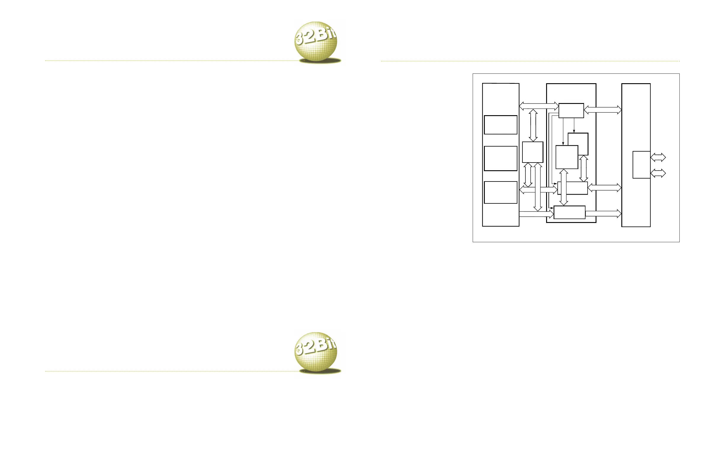
A modular, standard bus archi-
tecture separates the CPU core from on-chip peripherals. The
core communicates with on-chip memories using the tight-
ly coupled Kbus processor. This bus lets the core perform a
32-bit fetch from internal memory in one clock cycle by
pipelining the address and data. A controller interface on the
Kbus indirectly attaches the core to user-selectable cache,
ROM, and RAM modules. V3 uses a two-stage, but pipelined,
Kbus that adds one cycle to most operand-read accesses; how-
ever, the increased operating frequency offsets the extra
cycle. Another bus, the Mbus (master bus), offers centralized
arbitration. A special module connects the Mbus to the Kbus.
The Sbus (slave bus) interfaces to standard on- and off-chip
peripherals and attaches to the Mbus through a system-bus
controller.
On-chip debugging supports real-time trace; real-time and
non-real-time debugging; and access to control registers to
define types of memory regions, such as cacheable copy-back,
write-through, and noncacheable. Real-time trace reflects the
processor’
s status and indicates events such as instruction
completion and monitoring change-of-flow target addresses.
Real-time debugging supports program-counter-relative,
operand-address, operand-data, and non-real-time-debug
-
ging hardware breakpoints. Non-real-time debugging is sim
-
ilar to background-debugging mode on current 683xx prod
-
ucts. Y
ou can use a three-pin serial interface in this mode to
read register contents, generate an infinite-priority interrupt,
and for
ce the CPU to halt.
Power management: A low-power-stop (LPSTOP) instruc
-
tion shuts down active cir
cuits in the processor and halts
instruction execution. Processing resumes via a reset or valid
interrupt.
Special instructions: ColdFire added 32332-bit integer-
multiply, register-sign-extension, and multiword nonopera-
tion instructions to the 68000 architecture. Compilers use
nonoperation instructions to remove branch instructions.
Special on-chip peripherals: The MCF5200M processor,
which Motorola designed with its FlexCore methodology,
integrates the ColdFire core, debugging module, and mis-
alignment module with a multiply-accumulate (MAC) unit
supporting 16- and 32-bit operations. The MCF5202 supports
a 32-bit multiplexed bus with dynamic bus sizing that allows
access to 8-, 16-, or 32-bit memory and peripherals. It also has
a debugging module that provides serial control and visibili-
ty of the processor and memor
y system. Motorola offers the
ColdFire2 and ColdFire2M in the FlexCore library for cus
-
tomer design. Both devices integrate the ColdFire core with
a debugging module; a misalignment module; and memor
y
controllers that support as much as 32 kbytes each of RAM,
ROM, and instruction cache. The ColdFire2M also incorpo
-
rates the MAC unit.
Development tools: Third-party tools for the ColdFire fam-
ily include in-cir
cuit emulators from Embedded Support
T
ools (www.estc.com), Lauterbach (www
.lauterbach.com),
Microtec International (www
.microtec.com), Noral Micro-
logics (www
.noral.com), and Orion (www.yokogawa.com).
Cygnus (www
.cygnus.com), Diab Data (www.diabdata.com),
and Software Development Systems (www
.sds.com) offer C
compilers. W
ind River (www.windriver
.com), Integrated Sys-
tems Inc (www
.isi.com), Embedded System Products
(www
.esphou.com) offer ColdFire RTOS products. Hewlett-
Packard (www
.hp.com) offers preprocessor support.
Second sources: There are no second sour
ces for ColdFire.
EDN S
EPTEMBER
24, 1998
b 147
146 b EDN S
EPTEMBER 24, 1998
The Mitsubishi M32Rx/D contains a 32-bit RISC CPU; as
much as 4 Mbytes of on-chip DRAM, which Mitsubishi calls
“eRAM”; a 32316-bit multiply-accumulate (MAC) unit; and
a bus-interface unit (BIU). A 128-bit, 66-MHz internal bus
connects the CPU, DRAM, cache, and BIU. The M32Rx/D’s
circuitry automatically refreshes the internal DRAM.
The M32Rx/D family comprises the M32R/D and the new
superscalar M32Rx/D architectures. Both architectures are
instruction-set-compatible and comprise a combination of
16- and 32-bit-wide instruction formats with six addressing
modes. The devices include 16 32-bit, general-purpose regis-
ters and two 56-bit accumulators.
The M32R/D CPU executes most instructions in one clock
cycle, using an instruction-fetch, decode, execute, memor
y-
access, and write-back pipeline. The decode stage dispatches
instructions in order, and the remaining stages execute them
out of order to hide memory-access latency. The MAC unit
contains a single-cycle, 32316-bit multiplier and a 56-bit
adder.
The M32Rx/D contains a dual-issue, six-stage pipeline and
performs out-of-order execution; it can execute two 16-bit
instructions in parallel. The pipelines are asymmetrical, and
instructions have to align properly to keep the pipes full. For
example, both pipelines can execute arithmetic and logical
operations, but only Pipeline 1 can execute load/store and
jump/branch instructions. Additionally, only Pipeline 2 can
execute MAC instructions.
Both CPUs have an instruction queue of two 128-bit
entries. The cache maps directly to the address space and has
caching modes for internal instruction and data, for internal
and external instructions, and for cache off. If a cache miss
occurs, the CPU fetches one 128-bit data line in five cycles.
The BIU has 128-bit data buffers and supports burst transfers
on 128-bit boundary data.
A 16.67-MHz bus clock and four digital PLLs generate the
internal 66-MHz clock. The PLL contains a digital frequency
multiplier. Four cascaded, 64-tap inverter chains generate
four timing edges in one-half of a clock cycle. A phase detec-
tor and an up/down counter adjust the pulse width to one-
fourth of the one-half clock cycle to keep the duty cycle of
the four-times clock at 50%. The generated clock then feeds
into a digital phase shifter to reduce the phase difference
between the external and internal clocks to 400 psec.
Power management: The M32Rx/D supports sleep and
standby modes, during which the average power consump-
tion is 170 and 2 mW for the two modes, respectively, for the
2-Mbyte version. In the sleep mode, the CPU and caches stop;
in standby mode, only the DRAM is clocked.
Special instructions: The M32Rx/D supports MACs of
32316 and 16316 bits. It also performs data rounding in the
accumulator and block moves. The M32R/D and M32Rx/D
support 83 and 95 instructions, respectively. The M32Rx/D’s
additional instructions include five DSP-function instruc-
tions for MAC and rounding operations.
Special off-chip peripherals: Mitsubishi’s M65439FP
peripheral-function “super-I/O” chip performs such func-
tions as M32000D bus control, DRAM control supporting two
banks and page-mode burst transfers, and chip-select control
for as many as five 64-kbyte to 4-Mbyte blocks with one to
eight wait states. The peripheral I/O ASIC also contains a two-
channel DMA controller that can transfer as much as 2
Mbytes using cycle-steal, single-transfer, continuous-burst-
transfer mode or cycle-steal, continuous-transfer mode. An
interrupt controller handles 20 sources with priority resolu-
tion for as many as seven levels. Other functions of the
M65439FP include timers, a two-channel UART, and a two-
slot IC-card controller. The device sells for $8 (10,000).
Development tools: Cygnus (www.cygnus.com) supplies C
and C++ compilers and debuggers for the M32Rx/D. Mit-
subishi also supplies a C compiler and debugger, an evalua-
tion board, and an in-circuit emulator. Wind River
(www.windriver.com) supplies the Tornado development
environment, which includes the VxWorks RTOS. Integrated
Systems (www.isi.com) supplies the Prism+ development
environment, which includes the pSOS RTOS, Diab Data’s
(www.diabdata.com) C compiler and Light Source debugger.
Second sources:There are no second sources for the M32R/D
or M32Rx/D.
See EDN Web-site version, www.ednmag.com, for block
diagram.
Motorola’
s ColdFire, or VL-RISC (variable-length RISC),
ar
chitecture evolved from the M68000. VL instructions help
to attain higher code density
. Also, the ColdFire architecture
eliminates M68000 instructions, which embedded applica
-
tions rarely use, and optimizes the pipeline. As a result, it has
fewer transistors—approximately 55,000—than the M68000.
ColdFire continues to use the M68000 programmer’
s model.
Motorola designed three versions of ColdFire. The first ver
-
sion was relatively short-lived. The version 2 and 3 ar
chitec-
tures comprise two decoupled subpipelines: an instruction-
fetch pipeline (IFP) and an operand-execution pipeline
(OEP). An instruction buffer separates the two pipelines and
minimizes pipeline stalls. Motorola’
s design goals for V2
included making the core as small as possible. Hence, V2’
s IFP
is a simple two-stage pipeline: instruction-address generation
and instruction fetch.
Design goals for V3 were to stretch the pipeline to allow
the device to operate at clock frequencies of 90 MHz and
Mitsubishi M32Rx/D
Mot
orola ColdF
ire