164 b EDN S
EPTEMBER 24, 1998
Socket 7 processors, primarily characterized by a common
interface between the L2-cache bus and the main system bus,
are available from AMD, IBM, Integrated Device Technology
(IDT), Intel, Cyrix/National Semiconductor, and Rise Tech-
nology (www.rise.com). The common interface typically lim-
its the bus’s clock speed; however, some of these vendors
recently increased the bus speed from 66 to 100 MHz, effec-
tively boosting the bandwidth by 50%. One other way
around the bandwidth limitation is to put the L2 cache on
chip; AMD and IDT plan to take this approach this year.
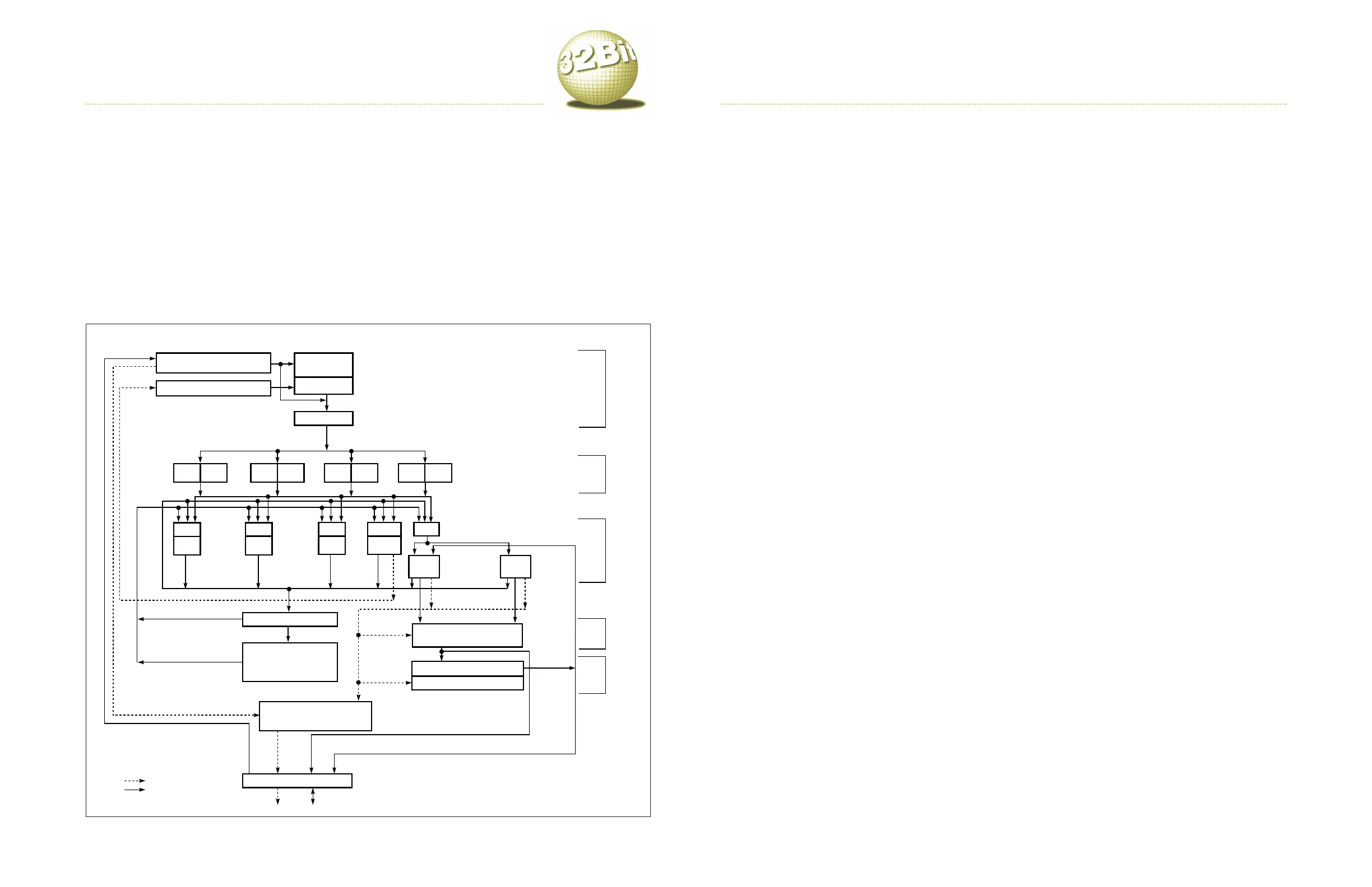
Intel’s Pentium processor, the first Socket 7 processor,
emphasizes executing simple instructions before complex
ones. With Pentium, the simple, RISC-like register-to-register
instructions drive the implementation; the microcoded com-
plex instructions are second priority
.
Pentium achieves a two-instruction issue peak and has two
five-stage pipelines (U and V) for each instruction. A com-
mon instruction fetch/align stage, which fetches multiple
instructions from the cache, feeds the U and V pipelines. The
CPU passes a full 256-bit line to the instruction decoder. Each
pipeline has two decoder stages to decode simple and com-
plex instructions. The wide cache-to-decoder path with two-
stage decoding enables Pentium to decode the x86’s variable-
length instructions.
Pentium includes 57 instructions to support multimedia
applications, such as image processing and audio synthesis.
More fundamentally, these multimedia-extension (MMX)
instructions benefit applications with vectorizable code.
Eight 64-bit MMX registers, MM0 to MM7, support these
instructions and data types; these registers are “aliased”—
physical silicon is the same but the registers’ names change—
with the floating-point registers. Register aliasing eliminates
additional silicon for new registers. It also eliminates the need
to modify the operating system or system BIOS, which must
Socket 7 processors
EDN S
EPTEMBER
24, 1998
b 165
track these registers. However, aliasing inhibits you from per-
forming routines that combine floating-point and MMX
instructions; switching from MMX instructions to floating-
point instructions can take as many as 50 clock cycles. Before
the CPU can execute a floating-point instruction, you must
use the empty-MMX-state instruction to set up the floating-
point registers.
For superscalar, dual-instruction, load/store operations,
the dual-ported Pentium data translation-look-aside buffer
(TLB) and cache tags provide concurrent pipeline accesses.
The eight-way-interleaved data-cache SRAM allows concur-
rent accesses to memory banks. (The cache is actually triple-
ported with an extra port for snooping.) Cache-hit rates range
from 90 to 97%, depending on the code mix. The data cache
handles both 4-kbyte and 4-Mbyte pages. It has two four-way,
set-associative TLBs, one with 64 entries for 4-kbyte pages and
one with eight entries for 4-Mbyte pages. The two-way, set-
associative code cache has a four-way, set-associative, 32-
entry TLB that handles both 4-kbyte and 4-Mbyte pages.
Dynamic branch prediction allows the CPU to determine
which branch to take. Pentium’s 256-entry branch-target
buffer (BTB) holds branch-target addresses for previously
executed branches. The BTB supplies the next instruction
address that the last execution of a branch instruction took.
Each BTB entry integrates the target address with history
and operation bits. Intel claims that a correctly predicted
branch takes one pipeline cycle and doesn’t cause a pipeline
bubble.
Pentium’s floating-point unit features an eight-stage
pipeline, which shares the first five stages of the U and V
pipelines. Data transfers to or from the FPU use a 64-bit-wide
datapath to the data cache. Pentium adds a write buffer to
each pipeline to avoid write contention.
Pentium uses burst reads to fill its 256-bit-wide cache line.
It also has burst write-back writes. The pipelined memory
interface allows a second bus cycle to set up while the first
bus cycle completes. Pentium reads or writes a 64-bit double
word each cycle in burst mode.
AMD’s K6-2 with MMX is a six-issue, superscalar mP with
a Socket 7-compatible bus interface that runs at 100 MHz. It
features a decoupled, decoding/executing, superscalar design
that can simultaneously decode multiple x86 instructions. It
also performs single-clock RISC operations, out-of-order exe
-
cution, data forwarding, speculative execution, and register
renaming. The K6-2 processor
, based on a six-stage pipeline,
contains parallel decoders, a centralized RISC86 operation
scheduler, and seven execution units.
Similar to the Pentium II, the K6-2 decodes x86 instruc
-
tions into RISC86 operations that adhere to the RISC-per
-
formance principles of fixed-length encoding, regularized
instruction fields, and a large register set. The K6-2 imple
-
ments branch-prediction logic in the form of an 8192-entr
y
branch-histor
y table, a branch-target cache, and a return-
address stack. In the K6-2, x86 instruction decoding begins
before the CPU fills the on-chip instruction cache. Predecod
-
ing logic determines x86-instruction length on a byte-by-
byte basis. The K6-2 stores this predecode information, along
with x86 instructions, in the instruction cache for later use
by the decoders. The decoders translate as many as two x86
instructions per clock into RISC86 operations.
The scheduler contains the logic needed to manage out-of-
order execution, data forwarding, register renaming, simul-
taneous issuing and retirement of multiple RISC86 opera-
tions, and speculative execution. The scheduler’s RISC86
operation buffer can hold as many as 24 operations. The
scheduler can simultaneously issue a RISC86 operation to
any available execution unit (store, load, branch, integer,
integer/multimedia, or floating point). The scheduler can
issue as many as six and retire as many as four RISC86 oper-
ations per clock.
Unlike the K6-2 (or Pentium II), Cyrix/National’s MII
processor directly executes native x86 instructions, rather
than converting x86 instructions into RISC-like instructions.
The MII achieves a dual-x86 instruction issue/execute rate
using dual seven-stage pipelines. The CPU performs register
renaming, multilevel dynamic branch prediction, specula-
tive execution, and out-of-order completion. The MII has a
dual-ported, 64-kbyte cache and a dual-ported, 384-entry
TLB; both support two reads and two writes or one read and
one write on every cycle. The processor allows you to turn
individual cache lines into scratchpad RAM to provide sup-
port for multimedia operations. In addition, the MII fully
supports Intel’s MMX instruction set.
The instruction-fetch stage of the MII’s pipeline fetches 16
instruction bytes per cycle from the instruction cache and
feeds the instruction-decode stage. The instruction decoder
issues as many as two complex x86 instructions per cycle.
During decoding, the decoder examines the resource require-
ments of the two instructions and chooses the optimal
pipeline for each instruction. During these stages, the
decoder accesses the 512-entry BTB and the 1024-entry
branch-history table to avoid pipeline bubbles.
During the access stages of the pipeline, the CPU performs
scoreboard checks, renames registers, and accesses the phys-
ical register file. The MII also calculates one or two linear
addresses per cycle for all addressing modes and accesses the
translation-look-aside and cache. The ability to fetch as many
as two memory operands from the data cache before the
instruction-execution stage allows the MII to execute mem-
ory-reference instructions in one cycle.
Cyrix’s Media GX processor with MMX performs all stan
-
dard north-bridge functions of a PC’s core logic. It also per-
forms the functions of the PC’s graphics controller
, audio
chip set, memor
y controller, and CPU-to-PCI bridge. Rather
than using only transistors to perform these functions,
Cyrix developed its V
irtual System Architecture (VSA). VSA
supports the graphics- and audio-hardware functions
through software. VSA uses the Media GX’s system-man
-
agement interrupt to capture any accesses to the memor
y-
or I/O-address ranges of the graphics and audio functions.
Once the processor enters system-management mode, it
executes Cyrix-supplied drivers to perform the appropriate
function.
Special instr
uctions:
MMX instructions operate on single-
instruction-multiple-data (SIMD) types. MMX instructions
include basic arithmetic operations, including add, subtract,
multiply
, and divide; logical operations, such as AND, OR,
and AND NOT
; compare operations; conversion instructions
to pack and unpack data elements; shift operations; and data-
movement instructions. AMD has developed 3-D instruction
extensions known as 3DNow
, which will also be implement-
ed by Cyrix and IDT
.
Socket 7 processors(continued)