XA User Guide 7-8 4/17/98
Figure 7.6 Typical External Code Read Using ALE
The following diagram shows a typical sequential code fetch where no ALE is issued between
code reads. Also note that the
PSEN bus control signal does not toggle, but remains asserted
throughout the burst code read
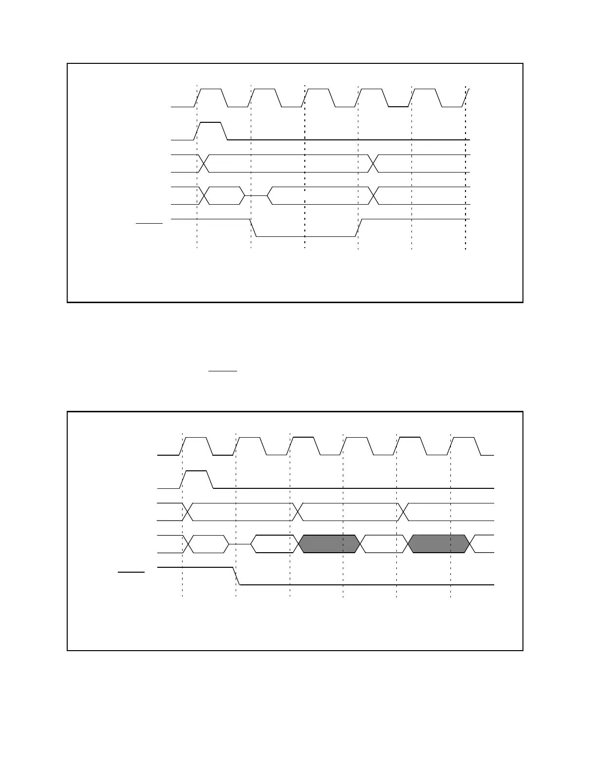
Figure 7.7 Burst Mode (Sequential) External Code Read
Note: the timing of this type of bus operation is user programmable. The timing shown
here is generated by the Bus Timing Register setup: ALEW = 0, CRA1/0 = 01.
Address/
Data bus
PSEN
Address bus
ALE
address
instruction data
XTAL1
Address/
Data bus
PSEN
Address bus
ALE
instruction
XTAL1
address
Note: the timing of this type of bus operation is user programmable. The timing shown here
is generated by the Bus Timing Register setup: ALEW = 0, CR1/0 = 01, CRA1/0 = 00.
data
instruction
data