4/17/98 7-9 External Bus
7.3.2 Data Memory
Reads and writes on the XA external bus are controlled through the use of the
RD, WRL, and
WRH signals. Since the XA bus supports both 8-bit and 16-bit widths, as well as byte and word
read and write operations, several different versions of the basic bus cycles are possible. These
are described in the following sections.
Data memory, like code memory, has a boundary where the internal data memory ends, and
above which the XA will switch to the external bus in order to act on data memory. This on/off-
chip data memory boundary may be in a different place for various XA derivatives, depending
upon the amount of internal data memory built into a specific derivative.
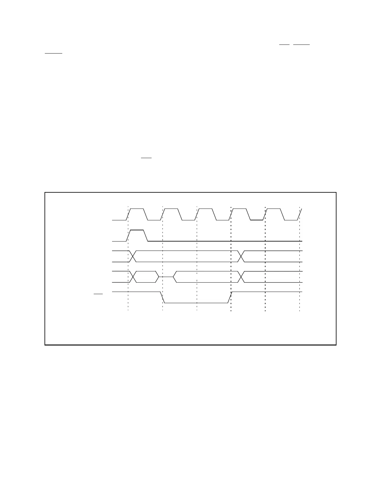
Typical Data Read
A simple byte read on an 8-bit bus or any read on a 16-bit bus both begin with an ALE cycle,
where the XA presents the address of the data location that is to be read on the bus. This is
followed by the assertion of the
RD strobe, that causes the external device to present its data on
the bus. This process is shown in the diagram below.
Figure 7.8 Typical External Data Read
Address/
Data bus
RD
Address bus
ALE
address
data in to XA
XTAL1
Note: the timing of this type of bus operation is user programmable. The timing shown
here is generated by the Bus Timing Register setup: ALEW = 0, DRA1/0 = 01.