4/17/98 7-11 External Bus
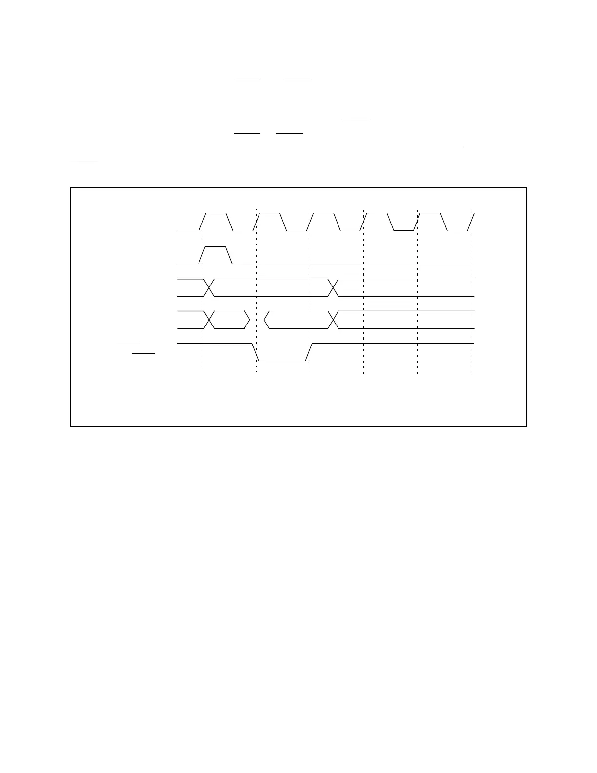
Typical Data Write
A data write operation begins with an ALE cycle, like a read operation, followed by the assertion
of one or both of the write strobes,
WRL and WRH. This simple bus cycle applies to byte writes
on an 8-bit data bus and all writes on a 16-bit data bus.
A byte write on an 8-bit data bus will always use only the WRL strobe. A byte write on a 16-bit
data bus will always use either the
WRL or WRH strobe, depending on whether the byte is at an
even or odd address. A word write on a 16-bit bus requires the assertion of both the
WRL and
WRH strobes. The simple data write cycle is shown below.
Figure 7.10 Typical External Data Write
Address/
Data bus
WRL and/or
WRH
Address bus
ALE
address
data out
from XA
XTAL1
Note: the timing of this type of bus operation is user programmable. The timing shown here
is generated by the Bus Timing Register setup: ALEW = 0, DWA1/0 = 00, WM0 = 0, WM1 = 0.