4/17/98 7-13 External Bus
External Bus Signal Timing Configuration
The standard XA bus also provides a high degree of bus timing configurability. There are
separate controls for ALE width, data read and write cycle lengths, and data hold time. These
times are programmable in a range that will support most RAMs, ROMs, EPROMs, and
peripheral devices over a wide range of oscillator frequencies without the need for additional
external latches, buffers, or WAIT state generators.
Programmable bus timing is controlled by settings found in the Bus Timing Register SFRs,
named BTRH, and BTRL, shown in Figures 7.12 and 7.13.
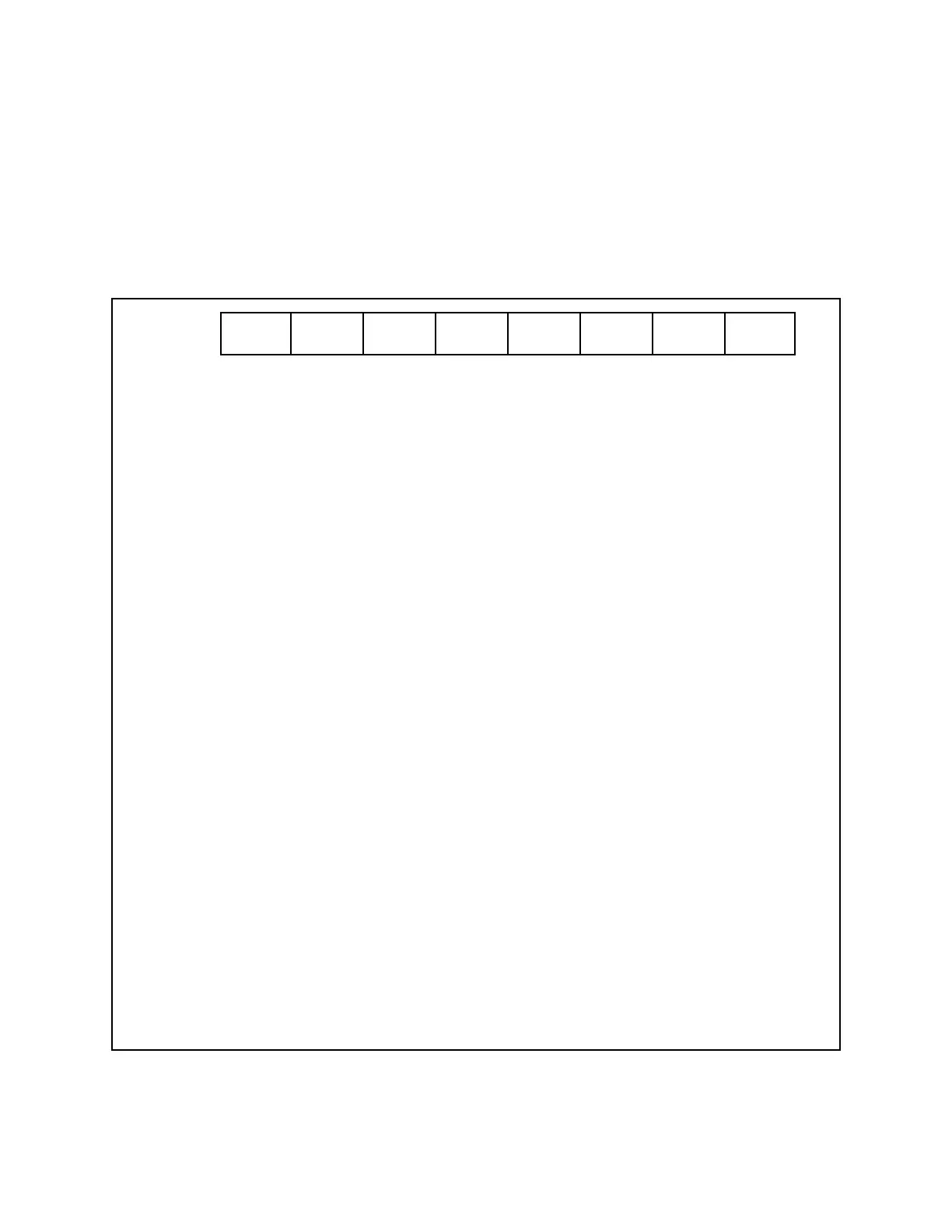
Figure 7.12 Bus Timing Register High Byte (BTRH)
DWA1 DWA0 DRA1 DRA0DR0DR1DW1 DW0
BTRH
DW1, DW0: Data Write without ALE. Applies only to the second half of a 16-bit write operation when
the bus is configured to 8 bits.
00 : Data write cycle is 2 clock in duration.
01 : Data write cycle is 3 clocks in duration.
10 : Data write cycle is 4 clocks in duration.
11 : Data write cycle is 5 clocks in duration.
DWA1, DWA0: Data Write with ALE. Selects the length (in CPU clocks) of the entire data write cycle,
including ALE.
00 : Data write cycle is 2 clocks in duration.
01 : Data write cycle is 3 clocks in duration.
10 : Data write cycle is 4 clocks in duration.
11 : Data write cycle is 5 clocks in duration.
DR1, DR0: Data Read without ALE. Applies only to the second half of a 16-bit read operation when
the bus is configured to 8 bits.
00 : Data read cycle is 1 clock in duration.
01 : Data read cycle is 2 clocks in duration.
10 : Data read cycle is 3 clocks in duration.
11 : Data read cycle is 4 clocks in duration.
DRA1, DRA0: Data Read with ALE. Selects the length (in CPU clocks) of the entire data read cycle,
including ALE.
00 : Data read cycle is 2 clocks in duration.
01 : Data read cycle is 3 clocks in duration.
10 : Data read cycle is 4 clocks in duration.
11 : Data read cycle is 5 clocks in duration.
Notes:
- See text regarding disallowed bus timing combinations.
- The bit pairs DW1:0, DWA1:0, DR1:0, DRA1:0, CR1:0, and CRA1:0 determine the length of entire
bus cycles of different types. Bus cycles with an ALE begin when ALE is asserted. Bus cycles without
an ALE begin when the bus strobe is asserted or when the address changes (in the case of burst
mode code reads). Bus cycles end either when the bus strobe is de-asserted or when data hold time
is completed (in the case of a data write with extra hold time, see bit WM0).