11
4.0 Addressing the 82C59A
There are two factors that must be taken into account when
addressing the 82C59A in a system. To begin with, the
82C59A is accessed only when the
CS pin (chip select) sees
an active signal (low). This signal is generated using control
circuitry in the system. Secondly, the various registers within
the 82C59A are selected based upon the state of the A0
(address pin) as well as specific bits in the command words
(i.e. for ICW1, OCW2, and OCW3 A0 must be a zero).
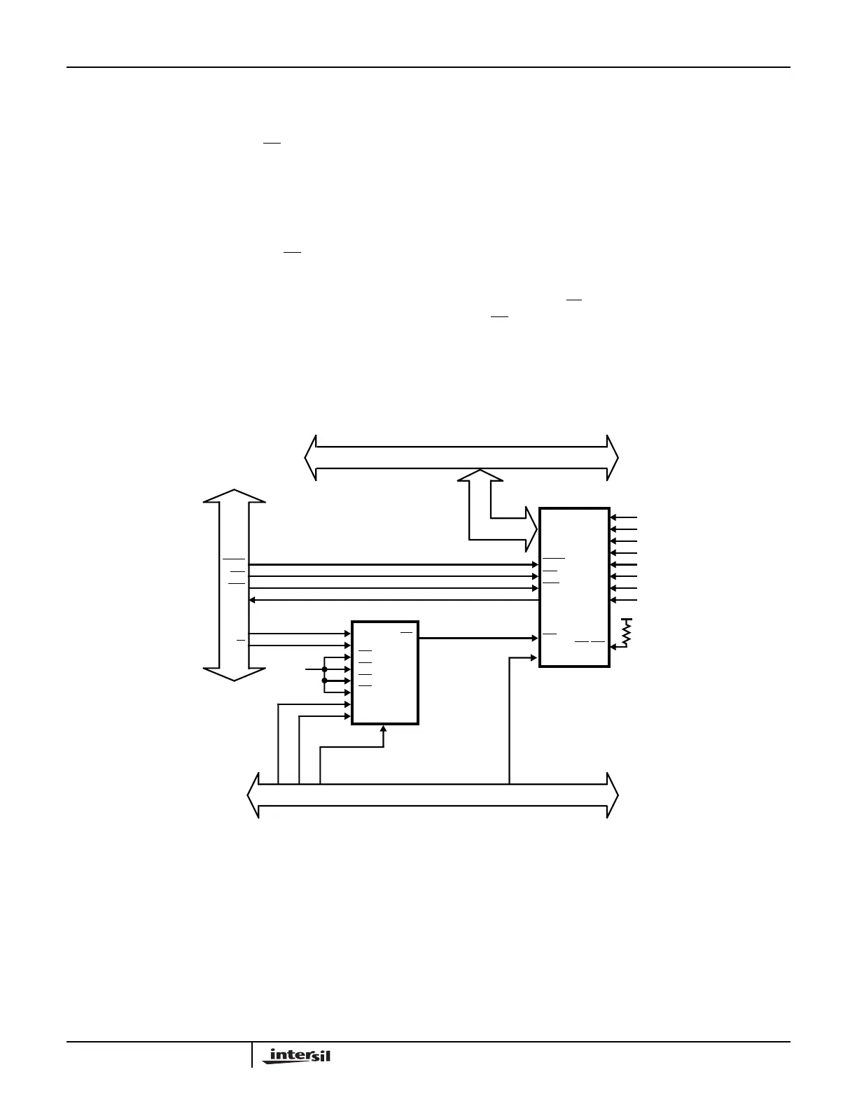
The circuit in Figure 15 shows that the
CS signal is
generated using an HPL-82C338 Programmable Chip Select
Decoder (PCSD). This device is being used as a 3-to-8
decoder. Note that the G1 input is active high and G2 thru
G5 have been programmed to be active low. The A, B, and C
inputs to the 82C338 correspond to address lines AD2, AD3,
and AD4 respectively, from the 80C88. The A0 input to the
82C59A is also taken from the CPUs address bus: AD0 is
used. It should be noted that address line AD1 from the
80C88 is not being used in the addressing of this particular
peripheral. This is done to allow other peripheral devices
that require two address inputs for internal register selection,
to use address lines AD0 and AD1 from the processor.
Because the AD1 address line from the 80C88 is not being
used, the 82C59A will be addressed regardless of whether
AD1 is high or low (1 or 0). The remainder of the address
lines from the 80C88 can either be a zero or one when
addressing the 82C59A. For the examples to be presented,
it can be assumed that all unused address lines will be set to
zero when addressing the 82C59A.
In Figure 15, output
Y6 from the HPL-82C338 is being used
as the
CS input to the 82C59A. This line is enabled when the
inputs on A, B, and C are: A = 0, B = 1, and C = 1.
Combining this with the A0 input to the 82C59A, we get the
addresses 18H and 19H for accessing the 82C59A.
FIGURE 15. ADDRESSING THE 82C59A
80C88 DATA BUS
INTA
RD
WR
INTR
ALE
IO/
M
IR3
IR2
IR1
IR0
IR4
IR5
IR6
IR7
SP/EN
A0
CS
INTA
RD
WR
INTR
VCC
2KΩ
D0 - D7
G4
G5
C
B
G3
G2
G1
ALE
Y6
A
82C338
82C59A
80C88 DATA BUS
AD0AD2AD3AD4
GND
80C88
CONTROL
BUS
Application Note 109