As you know, devices (or their controllers) contain various registers or ports that allow for
communication between the CPU and the device. The ports have a specific ordering, just as
memory locations do. To be able to read from or write to these ports, the designer must ensure
that the device is addressable. Each device must have a unique base address. This address
actually provides access to the first port on the device. Subsequent ports are accessible through
subsequent addresses. For example, assume that a particular device, such as the ACIA described
in Peripheral Devices and I/O, has four 8-bit ports. Suppose that the base address of the device is
0040h. The four ports on the device are then at 0040h, 0041h, 0042h, and 0043h. The ordering of
the ports (that is, which one is first, second, third, etc.) is part of the design of the device. The
data sheet for the device will give the relative port addresses (i.e., the offset for each port on the
chip).
We will work an example showing how to interface the Intel 8253 Programmable Interval Timer
(PIT) to an Intel 8088 chip. The timer is a device that we could use to count off the length of a
time slice for the kernel of a multitasking operating system. The timer has other uses as well, but
we will assume this particular application. The 8253 PIT includes three separate counters, each
of which is independently programmable. These are both input and output ports, that is the CPU
can both read from and write to these ports. The counters divide the input frequency by a given
number and counts down. When a counter reaches 0, it generates a pulse on the corresponding
output. If the GATE input (see below) for the counter is high, that is, the counter is still enabled,
it automatically restarts the count. The timer has a total of four ports, one for each counter
(Counter 0, Counter 1, and Counter 2) and a write-only control register. It also has some internal
registers that are not accessible to the programmer. The value in the control register determines
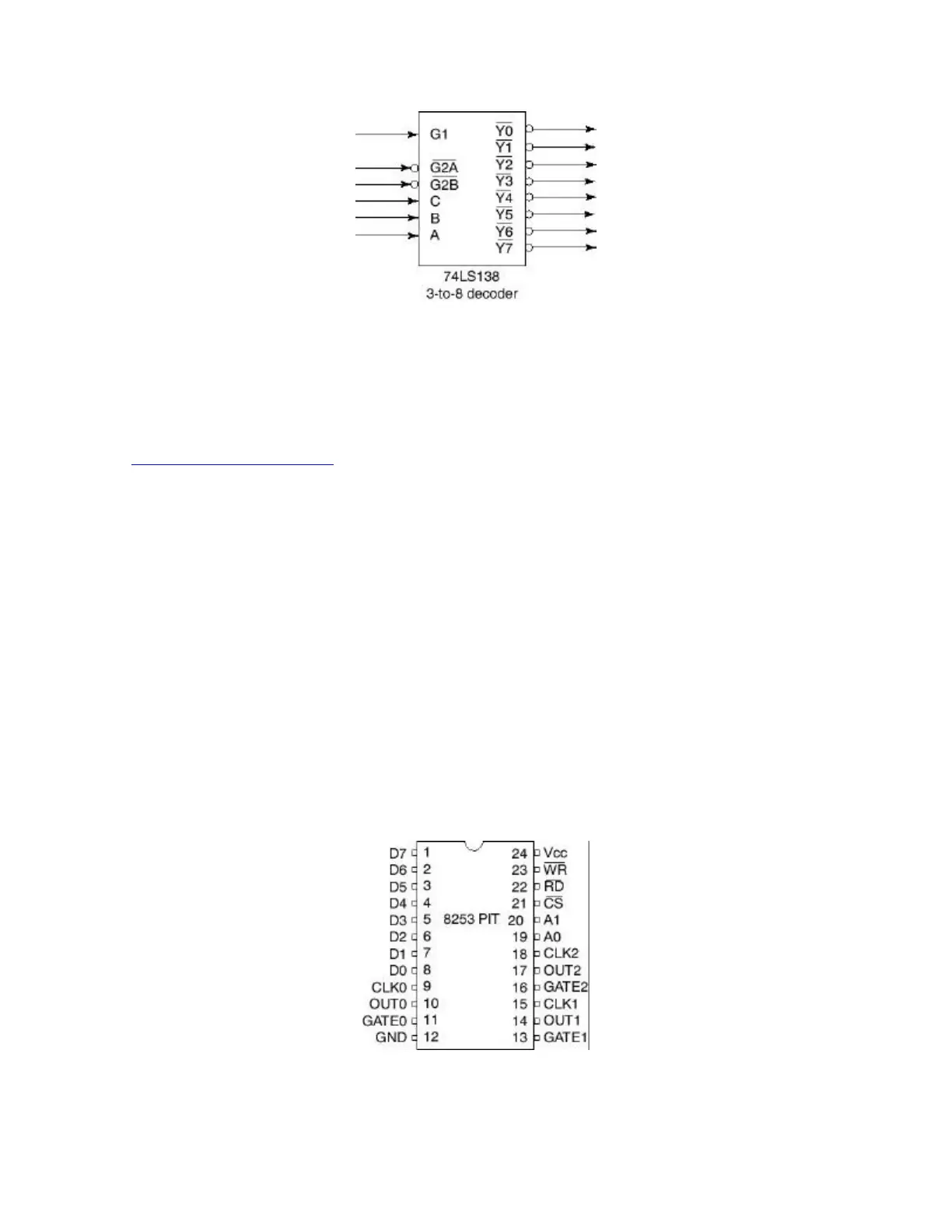
the mode of operation of the timer. The following figure shows the pin diagram for the 8253.
The general technique is to start with a known base address. For example, suppose you want to
connect the CS# pin of the 8253 timer to the Y0# line of the 74LS138 decoder so that the timer