has a base address of 80h. That is, we want the CS# pin of the timer to be active (low voltage)
only when the given address is 80h, 81h, 82h, or 83h. It should not be active for any other
address. The two low order bits of the address will give the addresses for the four ports on the
controller. These lines will connect directly to the timer, rather than to the decoder. This means
that we will route address bus lines A0 and A1 to the devices connected to the decoder. We can
use the next three higher order address lines (A2, A3, and A4) as the inputs to pins A, B, and C
of the decoder. Since the base address has all zeros in these bits (80h = 10000000
2
), connecting
these address lines directly to the input pins of the 74LS138 will have exactly the right effect.
We now have to account for address lines A5-A7. We have three gating signals on the decoder
that must be active if the decoder itself is to be active.
Since the 74LS138 is to serve as a connection strictly to I/O devices, one of the gating pins must
connect to the M/IO# control bus signal of the CPU, so that it is active only when an I/O
instruction (IN or OUT) is executing. Since this signal selects a chip when the line is low, it will
be simplest if we connect this line to one of the negative logic gating pins. We can arbitrarily
choose G2A#. In this way, if M/IO# is low (logic 0), G2A# will also be low and, provided the
other gating signals are also active, the decoder will be selected. Still remaining are pins G2B#
and G1. We will use address lines A5-A7 to activate these signals. When the address is 80h, the
values for these lines will be A7 = 1, A6 = 0, and A5 = 0. Of the two gating signals, G1 is active
high, so again, it makes sense to connect A7 directly to this pin. The last step is to combine lines
A6 and A5 so that only when both are zero, they will send a logic 0 to pin G2B#. To do this, we
invert both signals and connect them to a two-input NAND gate. Notice that the double inversion
(we first invert A5 and A6 and then get a second inversion from the NAND gate) is necessary.
Consider that we try to simplify this connection using no inversion at all. This means we would
connect lines A5 and A6 to a two-input AND gate. In this situation, we would get "false lows"
for certain addresses that would incorrectly activate the decoder and timer. Examine the
following truth table to see why (the starred entries show an incorrect result):
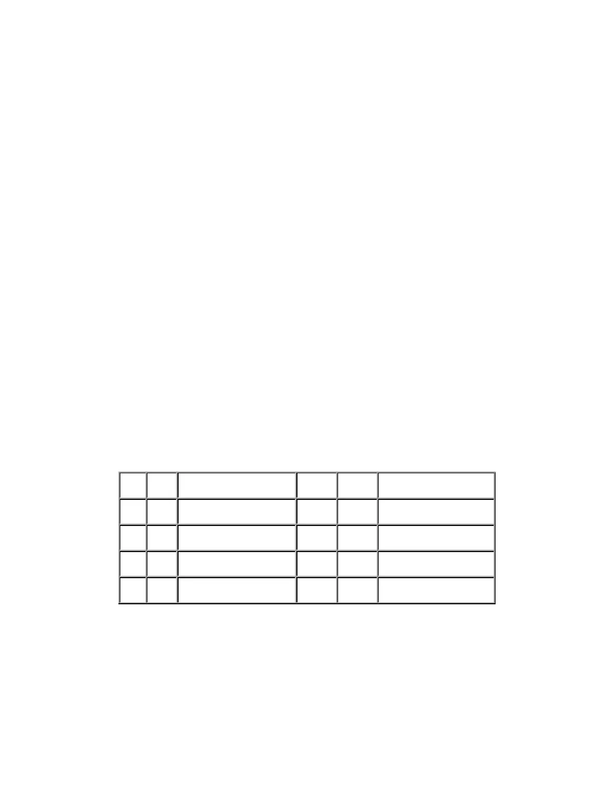
A5 A6 A5&A6 not A5 not A6 not (not A5 & not A6)
0 0 0 (G2B# active) 1 1 0 (G2B# active)
0 1 0 (G2B# active)* 1 0 1 (G2B# inactive)
1 0 0 (G2B# active)* 0 1 1 (G2B# inactive)
1 1 1 (G2B# inactive) 0 0 1 (G2B# inactive)
The following diagram shows the complete connection for the address lines (the x's represent
"don't cares," that is, bits for which the value is unimportant). You should try some other 8-bit
binary addresses with this connection scheme to convince yourself that no other address will ever
activate the Y0# line of the 74LS138 and thus the timer.