SDA Operator’s Manual
Vertical Noise Compensation
Introduction
Jitter is a measure of the timing error of data or clock signal transitions. The error is determined
by measuring the time at which the signal crosses a given amplitude level and comparing it to the
“expected” transition time. In a perfect world, this error would be entirely due to timing jitter but, as
is often the case, things are not so simple. All signals contain amplitude noise and this noise can
be interpreted as timing jitter in certain circumstances leading to higher overall jitter values. The
noise on the signal under test is, and should be, included in any jitter measurement, since the
data receiver would also interpret this as jitter. Any noise added by the test system should,
however, not be included as this will overestimate the jitter. The SDA includes a feature that
removes the system noise from the instrument, which uses the rms noise of the oscilloscope and
probe, if present. This section explains the theory of operation of the noise compensation.
Signal Slew Rate and How Vertical Noise Converts to Jitter
In RF electronics, this process is known as AM to PM conversion. The basic principle is that the
slew rate of the signal serves as a mechanism for vertical noise to be confused with horizontal
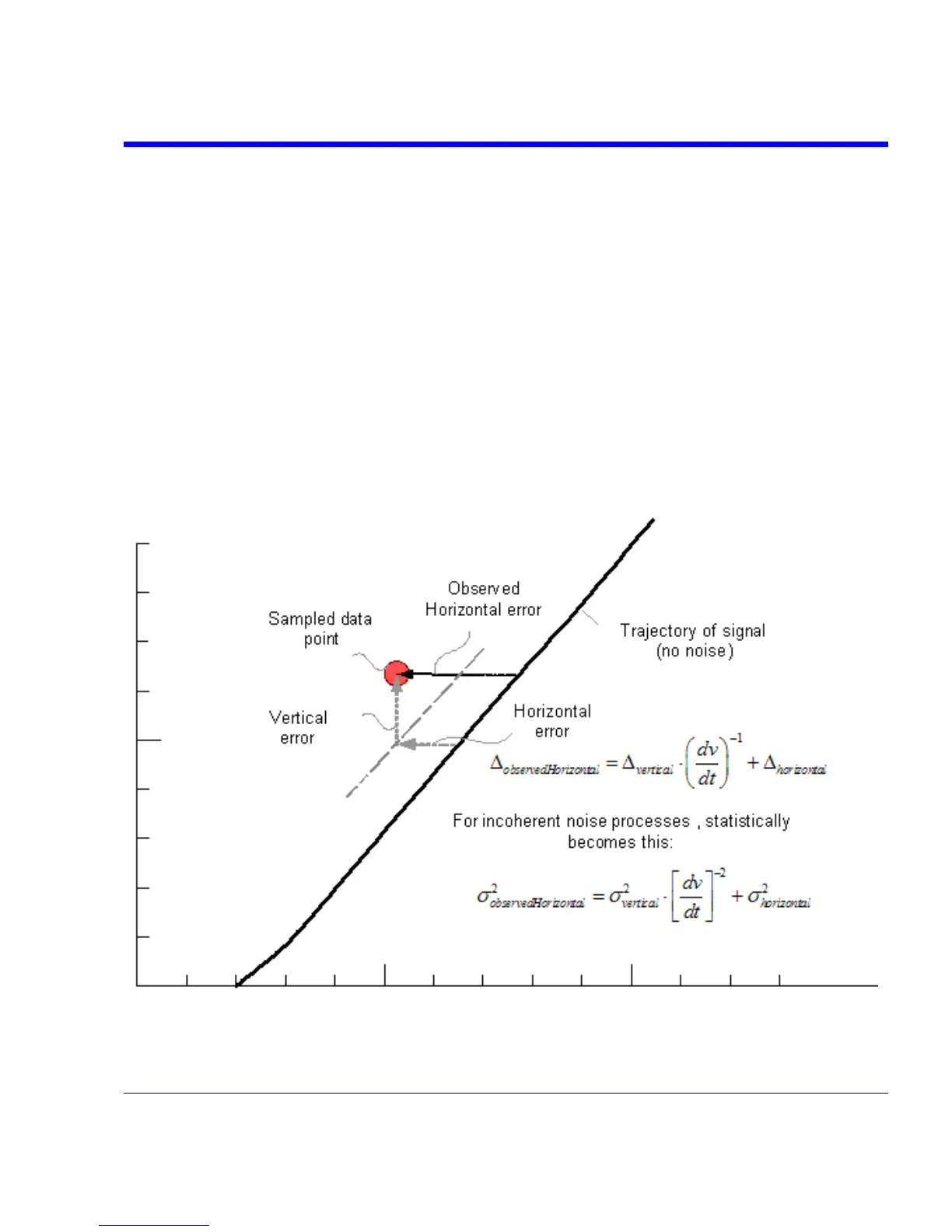
(timing) noise, and vice versa. The following image illustrates:
It is easy to see how if the slew rate is very high (i.e., very low rise-time) that the effect of vertical
noise is low and, conversely, that if the slew rate is very low, the vertical noise can dominate.
SDA-OM-E Rev H 385