FSB Theory of Operation
There are three sub-buses in the FSB: data bus, address bus, and common clock bus. All these
buses are bidirectional; information can flow in either direction. The direction of the bit flow will be
determined by the relative position of the high-to-low transition in the strobe pins (address, data
or clock) when simultaneously probed at both ends of the applicable bus. For example, when
signal A transition is delayed relative to signal B transition, this means that B is the transmitter
and A is the receiver. The bus clock (BCLK) signal is formed by a differential pair, BCLK0 and
BCLK1, running at 533 MHz. This is the trigger signal for the bit transactions, with the strobe
signals as the qualifiers for the actual bit transfers.
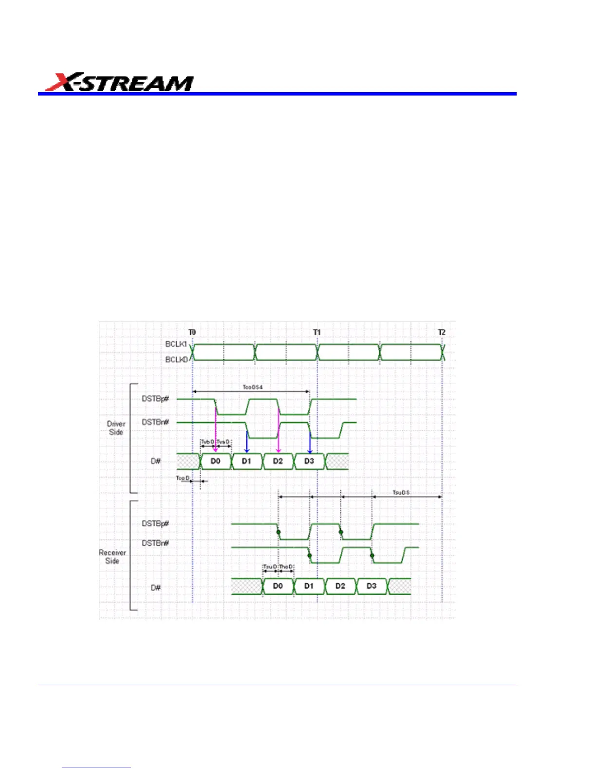
Data Bus Characteristics (Refer to Figure)
• During every period of BCLK, 4 bits are sent or there's an idle state: high voltage on both
strobes and relevant data pins.
• Bit transfers occur in quad multiples of bits only (4, 8, 12…).
• Data Strobe positive (DSTBp#) samples bits 0 and 2 on consecutive falling edges
• Data Strobe negative (DSTBn#) samples bits 1 and 3 on consecutive falling edges
Data Bus Timing Diagram ©Intel Corporation
360 SDA-OM-E Rev H