179
F3SG-R
User’s Manual
Chapter5 Input/Output Circuit
Input/Output Circuit and Applications
E
5-1. Input/Output Circuit
5-1-1. Entire Circuit Diagram
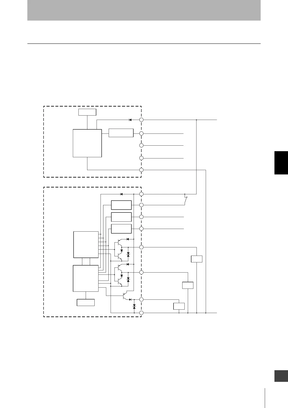
The entire circuit diagram of the F3SG-R is shown below.
The numbers in the circles indicate the connector's pin numbers.
5-1-1-1. F3SG-RA Series
PNP Output
2
1
5
8
7
6
+24 VDC
1
2
4
Brown
Black TEST
White Not used
Blue
Brown
White OSSD 2
Pink MUTE B
Gray MUTE A
Black OSSD 1
Red AUX
Blue
3
Reset input
circuit
4
Muting input
circuit B
3
Muting input
circuit A
Yellow RESET
0 VDC
5
Yellow Not used
Load
Indicator
Emitter
Main Circuit
Test Input
Circuit
Receiver
Main Circuit 2
Receiver
Main Circuit 1
Indicator
Load
Load

 Loading...